IGBT with back reinforcing structure and fabrication method thereof

A technology of enhanced structure and back injection, which is applied in semiconductor/solid-state device manufacturing, semiconductor devices, electrical components, etc., can solve the problems of reduced forward voltage and high forward voltage drop of IGBT

Inactive Publication Date: 2012-03-21
BYD CO LTD
View PDF8 Cites 13 Cited by
  • Summary
  • Abstract
  • Description
  • Claims
  • Application Information

AI Technical Summary

Problems solved by technology

[0006] In order to solve the technical problem of high forward conduction voltage drop of the existing IGBT, the present inventio...

Method used


Image

  • IGBT with back reinforcing structure and fabrication method thereof
  • IGBT with back reinforcing structure and fabrication method thereof
  • IGBT with back reinforcing structure and fabrication method thereof

Examples


Embodiment Construction

[0023] In order to make the technical problems, technical solutions and beneficial effects solved by the present invention clearer, the present invention will be further described in detail below in conjunction with the accompanying drawings and embodiments. It should be understood that the specific embodiments described here are only used to explain the present invention, not to limit the present invention.

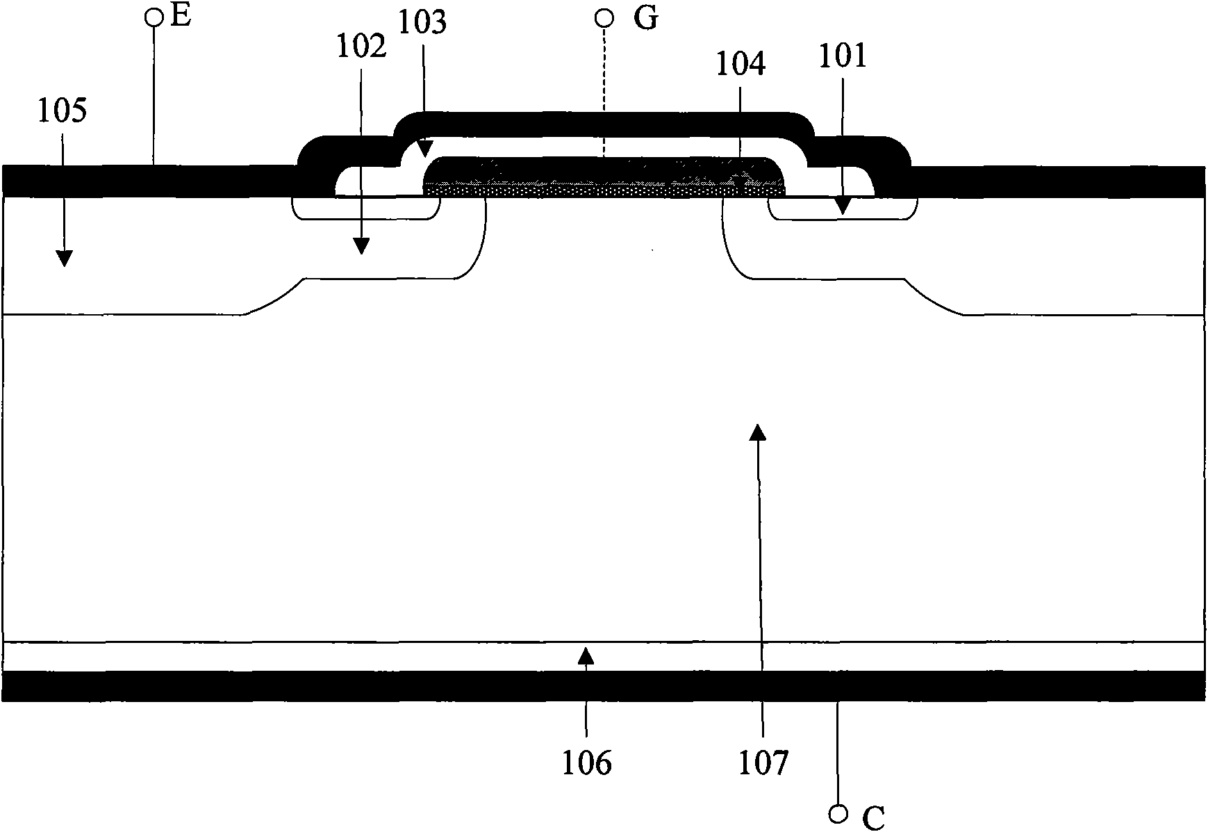
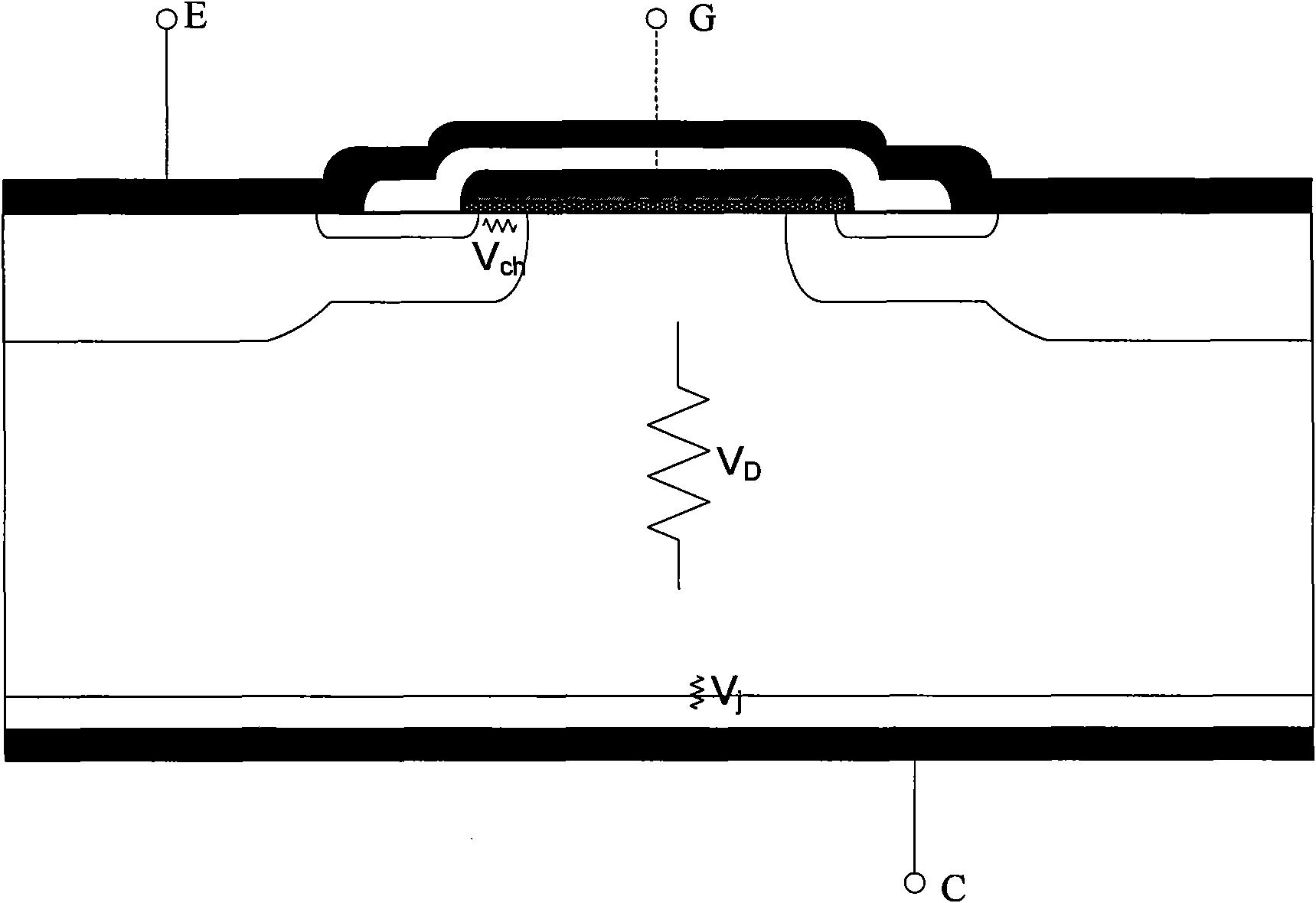
[0024] The conductance modulation effect in the IGBT is a phenomenon in which the conductance of the base region increases when the P+NP bipolar transistor operates under the condition of large injection, and it is also called the conductance modulation effect of the base region. For P+NP transistors, when the emitter junction voltage is large and a large number of minority carriers—holes are injected into the base region, there are correspondingly a large number of majority carriers—electrons in the base region. Caves have the same concentration gradient. This is equiv...


PUM


Abstract

The invention provides an insulated gate bipolar translator (IGBT) with a back reinforcing structure, and belongs to the transistor structure field. The uniform P+ typed collector regions of the traditional IGBT provided by the invention are changed into convex and concave structures, and the surfaces for contacting the P+ typed collector regions with N- typed shift regions are of convex and concave structures; the corresponding P+ typed collector regions and the collectors are also of convex and concave structures. In addition, the invention further discloses a fabrication method of IGBT with the back reinforcing structure. In the invention, as the surfaces of IGBT for contacting the N- typed shift regions and the P+ typed collector regions are of convex and concave structures, and the corresponding P+ typed collector regions and the collectors are also of convex and concave structures, the sizes of P and N junctions in the collector regions are enlarged and the purpose of reducing the positive connection voltage drop is achieved.

Description

technical field [0001] The invention belongs to the field of transistor structures, and in particular relates to an IGBT (Insulated Gate Bipolar Transistor, insulated gate bipolar transistor) with a back injection enhancement structure. Background technique [0002] IGBT is an important high-power switching device, and its forward voltage drop is one of the most important performance parameters of IGBT. Like all power switching devices, the voltage-current characteristics of the IGBT in the on-state determine its on-state power consumption, which is extremely important for determining the current handling capability. [0003] The structure of the IGBT device is derived from VDMOS (vertical double-diffused metal-oxide semiconductor field effect transistor). The IGBT device uses a P+ substrate to replace the N+ material in the VDMOS, but its cell structure is still very similar. The profile of an NPT-IGBT (non-punch-through IGBT) cell is as follows figure 1 shown. The surfa...

Claims


Application Information

Patent Timeline
IPC IPC(8): H01L29/739H01L29/08H01L21/331
Inventor 吴海平贾荣本
Owner BYD CO LTD
Why Eureka
Try Eureka