Conductive member and manufacturing method thereof

A technology for conductive parts and manufacturing methods, which can be applied to contact parts, electrical components, circuits, etc., and can solve problems such as hindering plating and electroplating, poor appearance, and reduced current efficiency.

Active Publication Date: 2012-03-28
MITSUBISHI SHINDOH CO LTD
View PDF10 Cites 10 Cited by
  • Summary
  • Abstract
  • Description
  • Claims
  • Application Information

AI Technical Summary

Problems solved by technology

[0021] (1) Mainly due to the relative velocity in the plating bath, a large amount of hydrogen gas is generated from the surface of the cathode when the plating is in progress, which hinders the plating performance of the plating, greatly reduces the current efficiency, and causes poor appearance (plating burn);
[0022] (2) As for multi-laye

Method used


Image

  • Conductive member and manufacturing method thereof
  • Conductive member and manufacturing method thereof
  • Conductive member and manufacturing method thereof

Examples


Example

[0077] (First embodiment)

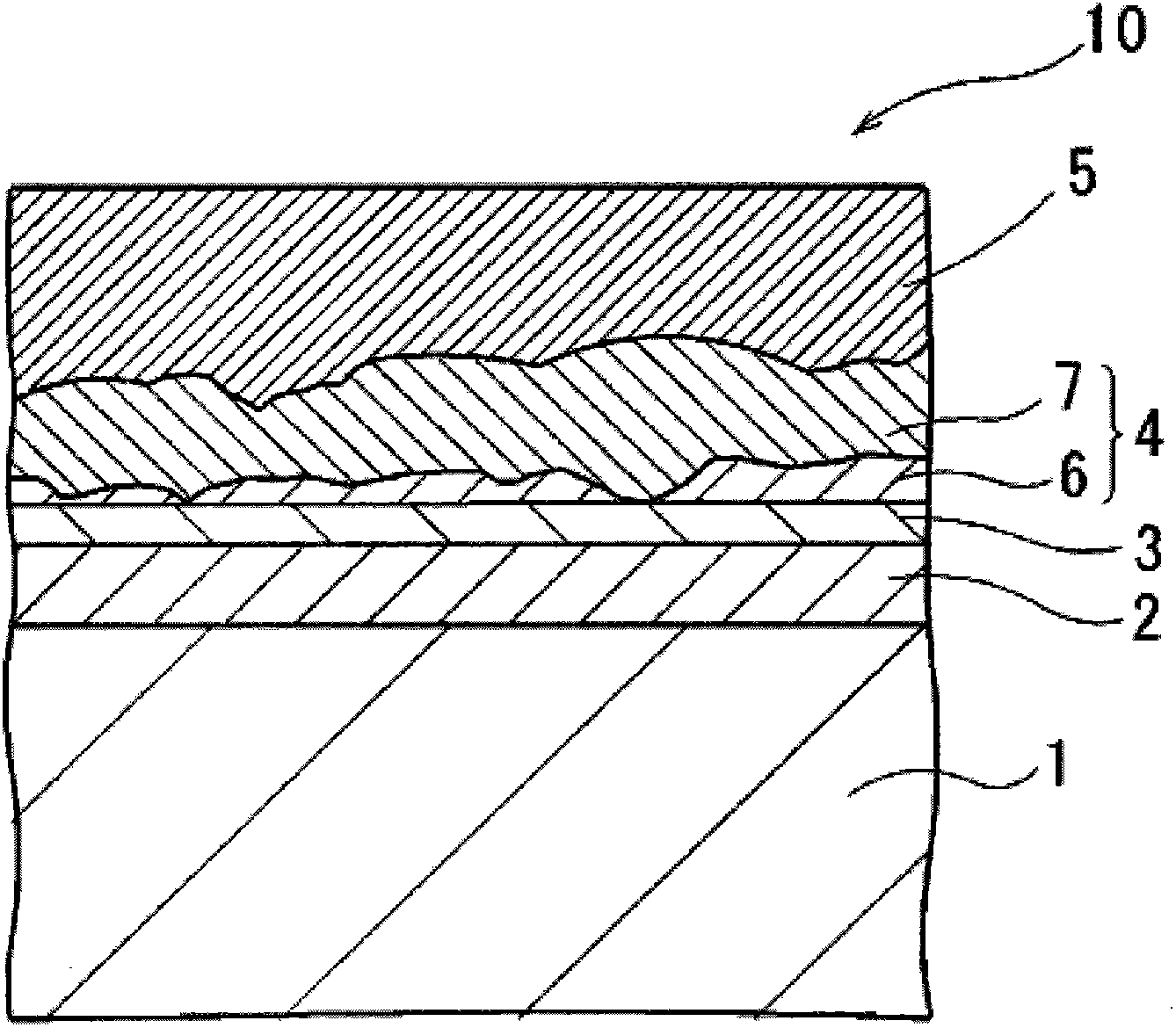
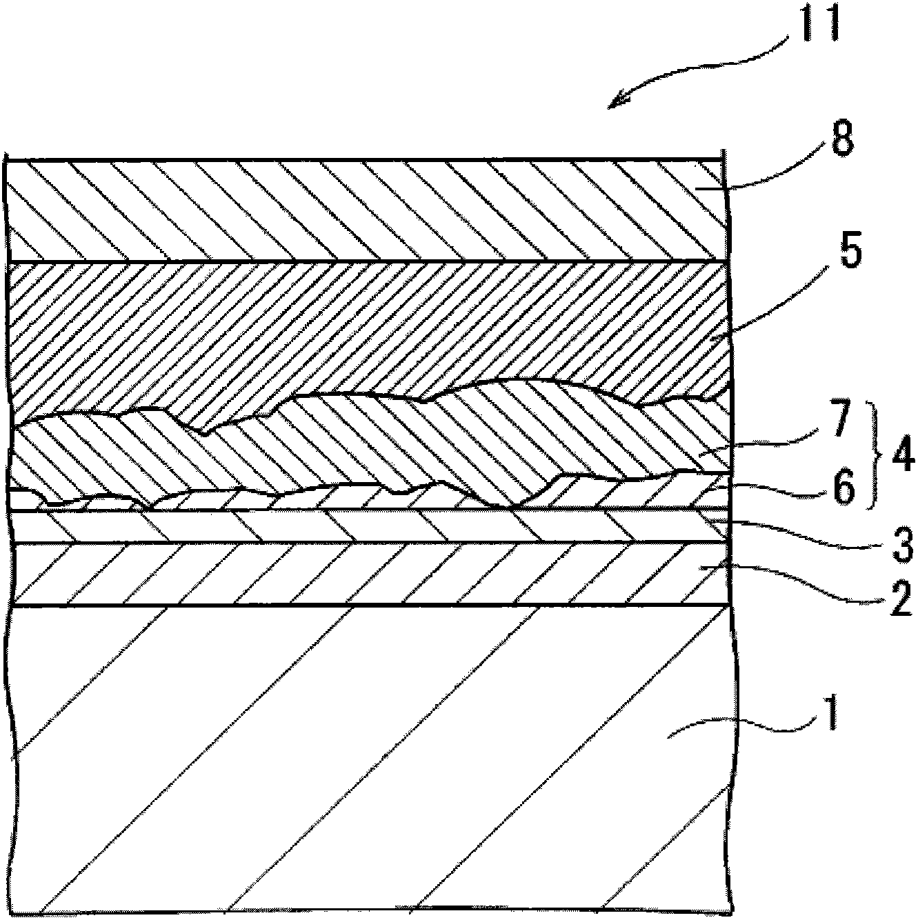
[0078] The conductive member 10 of the first embodiment is as figure 1 As shown, on the surface of Cu-based substrate 1, Ni-based underlayer 3, Cu-Sn intermetallic compound layer 4, Sn-based surface layer 5 are sequentially formed through Fe-based underlayer 2, and Cu-Sn intermetallic compound layer 4 Further by Cu 3 Sn layer 6 and Cu 6 Sn 5 Layer 7 constitutes.

[0079] The Cu-based substrate 1 is, for example, a plate-shaped substrate made of Cu or Cu alloy. As the Cu alloy, its material is not particularly limited, but Cu-Zn series alloys, Cu-Ni-Si series (Corson series) alloys, Cu-Cr-Zr series alloys, Cu-Mg-P series alloys are preferred , Cu-Fe-P-based alloys, Cu-Sn-P-based alloys, for example, MSP1, MZC1, MAX251C, MAX375, MAX126 manufactured by Mitsubishi Shindoh Co., Ltd. can be preferably used.

[0080] The Fe-based underlayer 2 is formed by electroplating Fe or Fe alloy, and is formed on the surface of the Cu-based substrate 1 to a thickness of ...

Example

[0124] (Second embodiment)

[0125] Next, the second embodiment will be described.

[0126] Figure 4 An example of a manufacturing apparatus that implements the manufacturing method of the second embodiment is schematically shown. The conductive member manufacturing apparatus 31 is continuously arranged with a degreasing washing tank 32, a Ni plating tank 33, a Cu plating tank 34, a Sn plating tank 35, and a washing tank 36 to 38 arranged after each plating tank 33 to 35, so that The copper strip 51 is continuously transported and plated in the order of the degreasing washing tank 32, the Ni plating tank 33, the Cu plating tank 34, and the Sn plating tank 35. The degreasing washing tank 32 is further composed of a degreasing tank 32a, a washing tank 32b, an acid washing tank 32c, and a washing tank 32d.

[0127] Moreover, the plating tanks 33 to 35 are as Figure 5 As shown, a pair of electrode plates 39 are arranged to be opposed to both surfaces of the continuously advancing cop...

Example Embodiment

[0159] [Example]

[0160] Next, an embodiment of the present invention will be described.


PUM

PropertyMeasurementUnit
Thicknessaaaaaaaaaa
Thicknessaaaaaaaaaa
Thicknessaaaaaaaaaa

Abstract

The conductive member has a stable contact resistance, resists peeling, displays a low insertion/removal force and is stable when used as a connector, and has an excellent fusing characteristic when used as a fuse. A Cu-Sn intermetallic compound layer (4) is formed between a Ni-based underlayer (3) formed on a Cu-based base material (1), and a Sn-based surface layer (5) that forms the surface. In addition, the Cu-Sn intermetallic compound layer (4) comprises a Cu3Sn layer (6) disposed on the Ni-based underlayer (3) and a Cu6Sn5 layer (7) that is disposed on the Cu3Sn layer (6). The surface roughness of the contact face between the Sn-based surface layer (5) and the Cu-Sn intermetallic compound layer (4) combining the Cu3Sn layer (6) and Cu6Sn5 layer (7) has an arithmetic mean roughness Ra of 0.05-0.25 [mu]m, and the maximum valley depth Rv of the roughness curve is 0.05-1.00 [mu]m. Furthermore, the Cu3Sn layer covers the Ni-based underlayer with a surface coverage of 60-100%.

Description

technical field [0001] The present invention relates to a conductive member for electrical connection connectors, fuses, etc., in which a plurality of plated layers are formed on the surface of a substrate made of Cu or Cu alloy, and a manufacturing method thereof. [0002] This application is based on Japanese Patent Application No. 2009-98043 filed in Japan on April 14, 2009, Japanese Patent Application No. 2009-115289 filed in Japan on May 12, 2009, and Japanese Patent Application No. 2009 filed in Japan on May 26, 2009. -127085 claims priority, the content of which is incorporated herein. Background technique [0003] Conductive parts such as connectors for electrical connection of automobiles and connection terminals of printed circuit boards are often used to plate Sn-based metals on the surface of Cu-based substrates composed of Cu or Cu alloys in order to improve electrical connection characteristics. conductive parts. [0004] Such conductive members include those...

Claims


Application Information

Patent Timeline
IPC IPC(8): C25D7/00C25D5/12C25D5/50H01H85/06H01R13/03
CPCC25D5/12H01R13/03C25D5/50C25D7/00C25D5/617
Inventor 樱井健石川诚一久保田贤治玉川隆士
Owner MITSUBISHI SHINDOH CO LTD
Why Eureka
Try Eureka