Matching detection method and circuit of content addressable memory cell

A technology for addressing memory and storage units, applied in static memory, digital memory information, information storage, etc., can solve the problems of large power consumption, consumption, waste of matching signal lines, etc., to reduce current consumption, reduce current consumption, reduce The effect of bias voltage and bias current

Inactive Publication Date: 2012-04-04
INST OF ACOUSTICS CHINESE ACAD OF SCI
View PDF5 Cites 6 Cited by
  • Summary
  • Abstract
  • Description
  • Claims
  • Application Information

AI Technical Summary

Problems solved by technology

[0008] From the above three traditional solutions, it can be seen that the initial discharge of the matching signal line still wastes a lot of power consumption; the use of current saving technology and positive feedback technology can reduce the charging current of the matching signal line in the state of content mismatch, but requires additional offset voltage and consume additional quiescent current in the control branch at the expense of

Method used


Image

  • Matching detection method and circuit of content addressable memory cell
  • Matching detection method and circuit of content addressable memory cell
  • Matching detection method and circuit of content addressable memory cell

Examples


Embodiment Construction

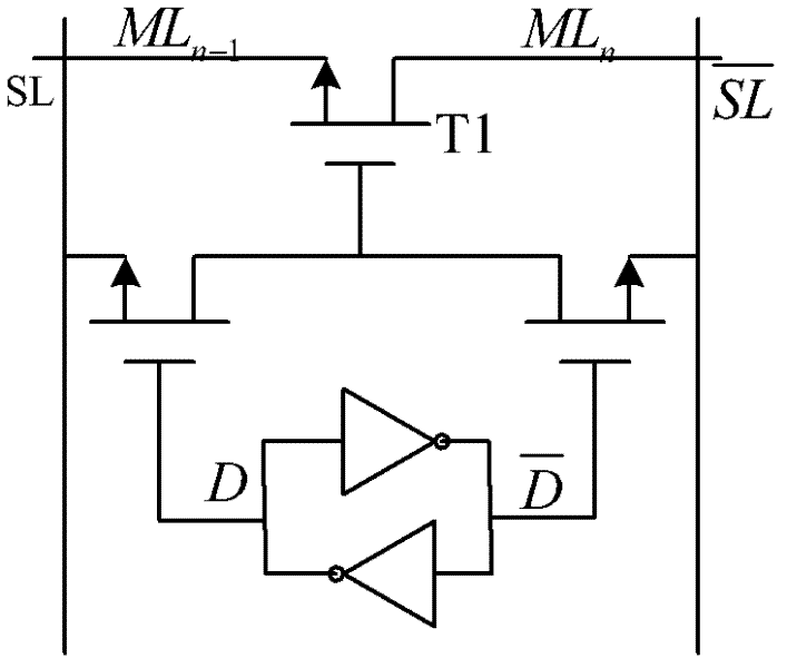
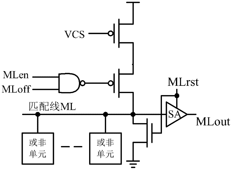
[0026] Specific embodiments of the present invention will be described in more detail below with reference to the accompanying drawings, Image 6 is a block diagram of an embodiment of the present invention or a non-memory cell matching detection circuit, Figure 7 Schematic diagram of yes or no memory cell matching detection circuit. Such as Image 6 As shown, the OR non-memory cell matching detection circuit includes: a pre-charge circuit, a charging circuit, a feedback control circuit, an equalization circuit, an OR non-memory cell, a sensitive amplifier (SA), a power supply and ground, wherein, the number of OR non-memory cells is greater than 1. The first matching signal line MLA and the second matching line signal MLB are formed by parallel connection of several NOR memory cells (hereinafter referred to as matching signal line MLA and matching line signal MLB).

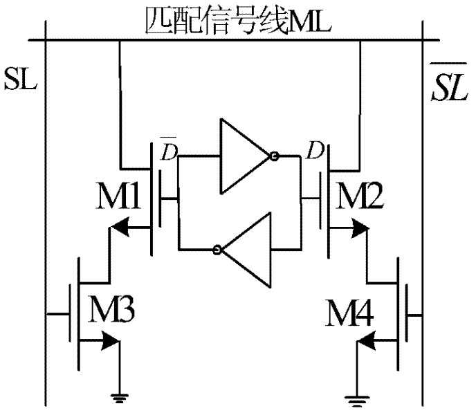
[0027] Such as Figure 7 As shown, the circuit transistors N1, N2, N3, N4, N5 and the OR non-memory cells ...


PUM


Abstract

The invention relates to a matching detection method and circuit of a content addressable memory cell. The matching detection method comprises the steps of: carrying out charging or charging control on a charge circuit of a first matching signal wire and a feedback control circuit of a second matching signal wire; when contents of an NOR memory cell are matched and a voltage difference exists between the matching signal wires, outputting a matching signal; and when the contents of the NOR memory cell are mismatched and no voltage difference exists between the matching signal wires, not outputting the matching signal. The matching detection method is simple and reliable, and has the advantages of reduction in additional offset voltage and offset current and further reduction in power consumption in comparison with the traditional matching detection method of the memory cell.

Description

technical field [0001] The present invention relates to a content addressable memory, in particular to a matching detection method and circuit of a content addressable memory storage unit. Background technique [0002] Content-Addressable Memory (CAM) is a content-addressable memory for specific high-speed search applications. Its working principle is: when the user provides a piece of data, CAM will traverse the entire storage space to search whether the data exists in the storage, and if so, CAM will return one or more addresses where the hit data exists. CAM is a special memory that searches the entire memory in a single operation. Therefore, in search applications, CAM is much faster than ordinary memory. The fast search feature of CAM makes CAM especially suitable for applications such as network equipment, central processing unit, and video hard codec. [0003] The storage unit structure of traditional content addressable memory is divided into NAND type storage uni...

Claims


Application Information

Patent Timeline
Patent Type & Authority Applications(China)
IPC IPC(8): G11C7/06G11C15/00G11C15/04
Inventor 闫浩洪缨王东辉侯朝焕
Owner INST OF ACOUSTICS CHINESE ACAD OF SCI
Why Eureka
Try Eureka