Method for thinning chip
A wafer and thinning technology, which is applied in electrical components, semiconductor/solid-state device manufacturing, circuits, etc., can solve problems such as cost increase and fragmentation, and achieve the effect of reducing production cost, avoiding fragmentation, and reducing the probability of fragmentation.
- Summary
- Abstract
- Description
- Claims
- Application Information
AI Technical Summary
Problems solved by technology
Method used
Image

Examples
Embodiment Construction
[0024] In order to enable those who are familiar with the technical field of the present invention to further understand the present invention, several preferred embodiments of the present invention are listed below, together with the accompanying drawings, to describe in detail the composition of the present invention and the intended achievement effect.
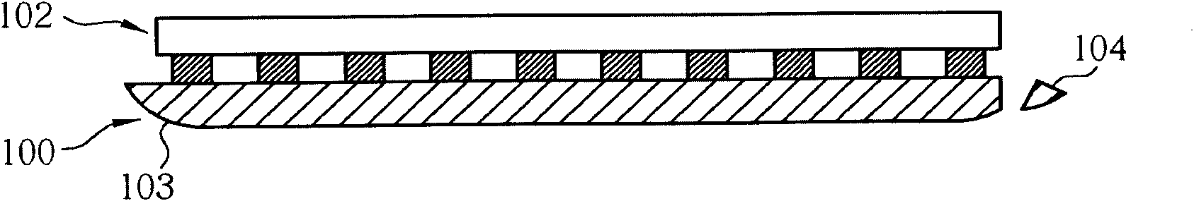
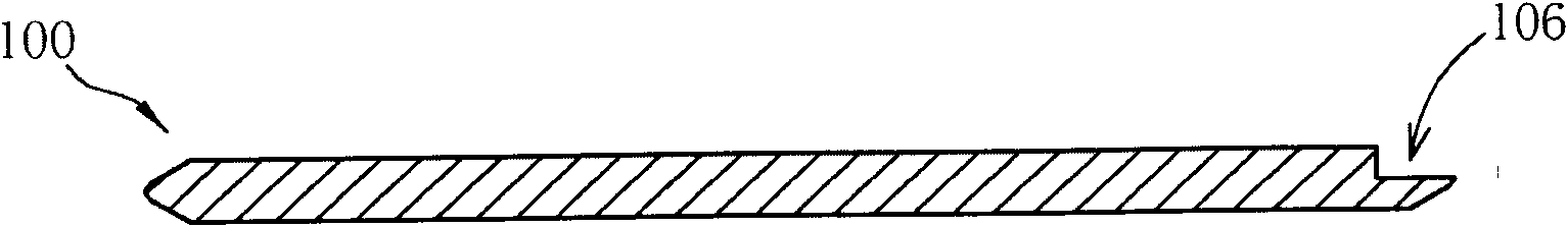
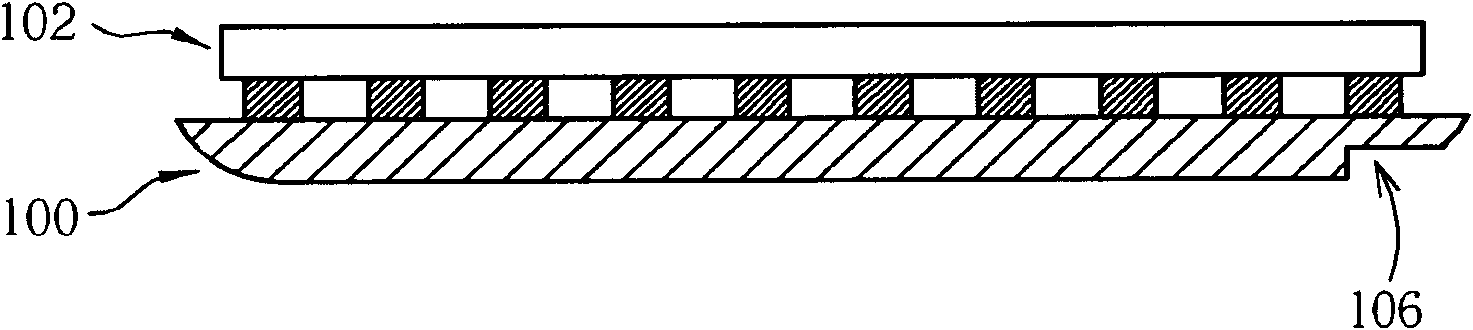
[0025] Please refer to Figure 4 to Figure 6 , is a schematic diagram of the steps of the wafer thinning method according to the first embodiment of the present invention. First, if Figure 4 As shown, a wafer 300 is provided. The chip 300 has an active surface 302 , a back surface 304 and a side surface 306 . There may be multiple semiconductor structures (not shown) on the active surface 302, such as metal oxide semiconductor (metal oxide semiconductor, MOS), complementary metal oxide semiconductor (complementary metal oxide semiconductor, CMOS), photodiode (photo diode) , a metal interconnection, a bonding pad, or a ...
PUM
 Abstract
Description
Claims
Application Information