Method of manufacturing thick copper foil PCB (Printed Circuit Board)

A technology of copper foil and copper foil thickness, which is applied in the manufacture of printed circuits, the manufacture of printed circuit precursors, the removal of conductive materials by chemical/electrolytic methods, etc. Achieve the effect of reducing the possibility of voids or pores, easy glue flow, and reduced glue flow depth

Inactive Publication Date: 2012-04-04
田先平
View PDF2 Cites 15 Cited by
  • Summary
  • Abstract
  • Description
  • Claims
  • Application Information

AI Technical Summary

Problems solved by technology

On the other hand, when the thickness of the copper foil increases, the glue flow depth of the prepreg increases during the lamination process of the multi-layer board, making it more difficult to fill the glue, and it is easy to form voids or pores inside the PCB.

Method used


Image

  • Method of manufacturing thick copper foil PCB (Printed Circuit Board)
  • Method of manufacturing thick copper foil PCB (Printed Circuit Board)
  • Method of manufacturing thick copper foil PCB (Printed Circuit Board)

Examples


Embodiment Construction

[0027] The method of the present invention will be further described by taking the manufacture of single-sided PCB as an example in conjunction with the accompanying drawings and preferred specific embodiments:

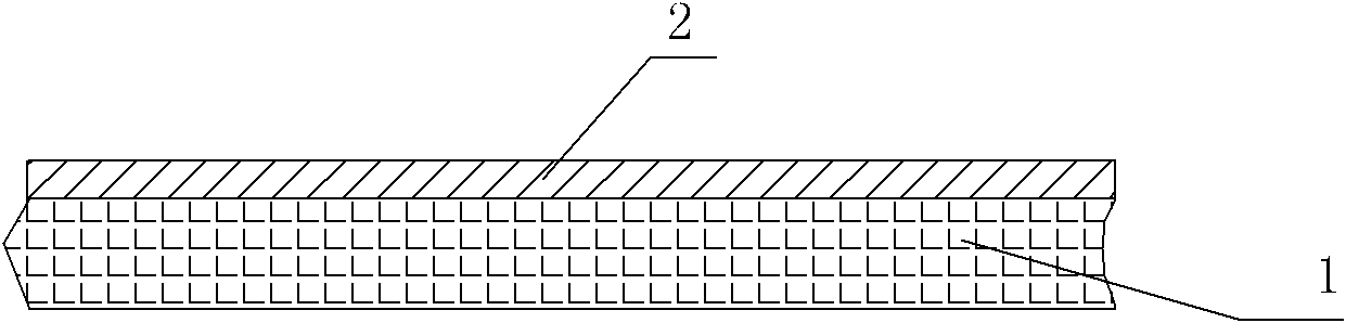
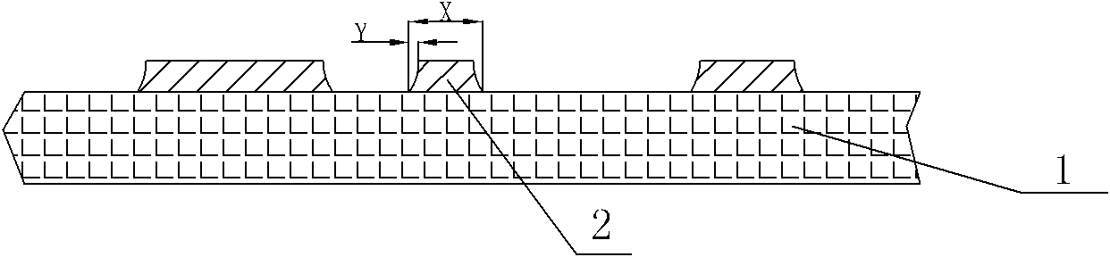
[0028] refer to figure 1 with figure 2 As shown in , the existing method manufactures single-sided PCBs, which are etched from single-sided copper clad laminates. Copper foil 2 is covered on one surface of the substrate composed of insulating medium 1, and a resist layer is made on the surface of copper foil 2 according to a circuit pattern, and copper foil 2 is directly etched until the etched area of ​​copper foil 2 is etched through. , to form a copper foil line. From the perspective of one of the copper foil lines, its design width is X, but after etching, a side etching amount Y is produced on the side of the copper foil, making the surface of the copper foil line obvious. Thinner, it has a greater impact on copper foil with thicker thickness or thinner width....


PUM


Abstract

The invention discloses a method of manufacturing a thick copper foil PCB (Printed Circuit Board) and relates to a manufacturing technology of a PCB. The technical problem that thicker copper foil degree leads to bigger influence caused by obviously thinning surface of a copper foil circuit due to large lateral erosion amount in the etching process is solved. The method comprises the following steps of: 1) producing an anti-corrosion layer on a front surface of a copper foil according to a designed circuit diagram and applying the anti-corrosion layer on the back surface of the copper foil for protection; 2) etching the copper foil and stopping the etching when the depth of an etching area of the front surface is larger than 1/3 and is smaller than 2/3 the thickness of the copper foil; 3) removing the anti-corrosion layers on the front surface and the back surface of the copper foil and adhering the front surface to an insulating medium in a pressing manner; 4) forming an another anti-corrosion layer on the back surface of the copper foil again, wherein the anti-corrosion layer on the back surface of the copper foil is a mirror image of the circuit diagram on the front surface of the copper foil; and 5) etching the copper foil again and stopping the etching when the etching area of the back surface and the etching area of the front surface are etched to penetrate each other. The etching thickness of the copper foil can be increased by one time under the condition that the etching amount is reduced by 50% or the same lateral etching amount is required.

Description

technical field [0001] The invention relates to a manufacturing technology of a printed circuit board (PCB), in particular to a manufacturing method for realizing a thick copper foil PCB. Background technique [0002] In the existing PCB manufacturing method, whether it is a single-sided board, a double-sided board, or a multi-layer board, the copper clad laminate that has been pressed and bonded to the insulating medium is used as the raw material, and the circuit pattern is first made on its surface. The corresponding anti-corrosion layer is then chemically etched. The PCB produced in this way generally has a thickness of copper foil below 2OZ (ounces). To make thicker copper foil, pattern electroplating must be used to increase the copper thickness, but the increased copper thickness is also limited, generally below 4OZ, and also greatly increases the production cost. Therefore, in actual production, there are very few PCBs with copper foil thickness above 4OZ. When thi...

Claims


Application Information

Patent Timeline
Patent Type & Authority Applications(China)
IPC IPC(8): H05K3/06H05K3/42
CPCH05K2203/0369H05K3/022H05K3/06H05K3/42
Inventor 田先平
Owner 田先平
Why Eureka
Try Eureka