Terminal protection structure of super-junction semiconductor device and fabrication method thereof

A terminal protection structure and semiconductor technology, which is applied in the direction of semiconductor devices, semiconductor/solid-state device manufacturing, electrical components, etc., to achieve high device withstand voltage characteristics, device withstand voltage improvement, and high reliability.

Active Publication Date: 2014-07-09
SHANGHAI HUAHONG GRACE SEMICON MFG CORP
View PDF4 Cites 0 Cited by
  • Summary
  • Abstract
  • Description
  • Claims
  • Application Information

AI Technical Summary

Problems solved by technology

[0004] The technical problem to be solved by the present invention is to provide a terminal protection structure of a super junction semiconductor device, which can improve the withstand voltage characteristics and reliability of the device without increasing the complexity of the process; therefore, the present invention also provides a A kind of fabrication method of super junction semiconductor device

Method used


Image

  • Terminal protection structure of super-junction semiconductor device and fabrication method thereof
  • Terminal protection structure of super-junction semiconductor device and fabrication method thereof
  • Terminal protection structure of super-junction semiconductor device and fabrication method thereof

Examples


Embodiment 1

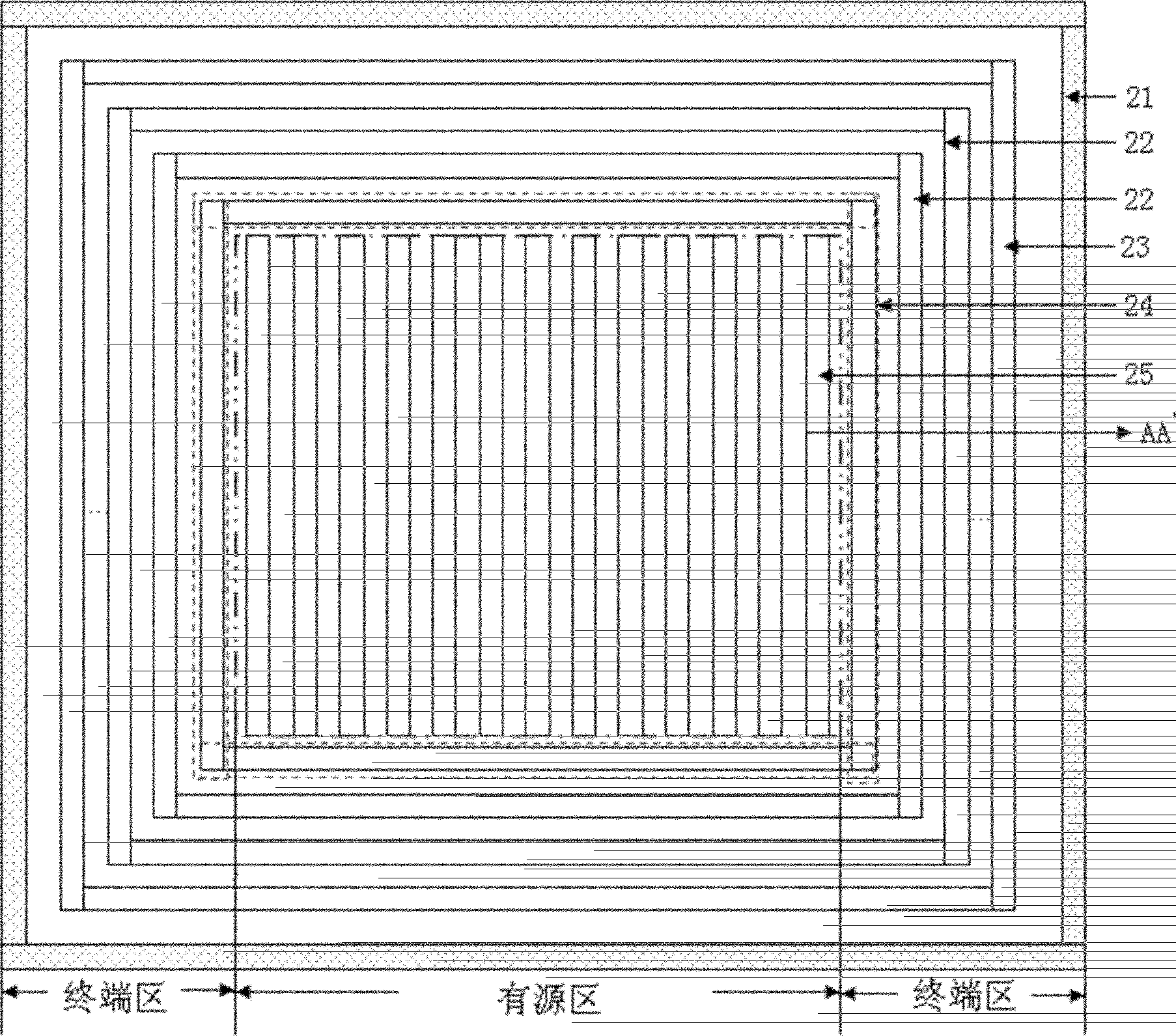
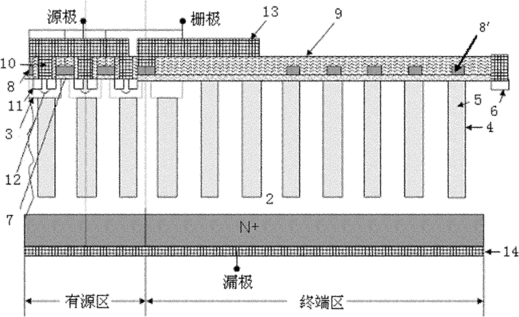
[0034] Embodiment one, see image 3 , 4 As shown, the terminal protection structure of the super junction semiconductor device in this embodiment includes: a channel stop ring 21 located at the outermost end of the terminal region, a P-type annular groove 23 located in the channel stop ring 21, and a channel stop ring 23 located in the channel stop ring 21. The P-type annular groove 22 (generally a plurality of grooves) inside the annular groove 23, the P-type ring 24 located in the P-type annular groove 22; the annular groove 23 has at least two depths Like the grooves, grooves 23 have at least two different depths from the set of grooves in grooves 22 . The active area trench 25 located in the active area is disposed in the P-type ring 24 . The channel stop ring 21 , the annular groove 23 , the annular groove 22 , and the P-ring 24 are all square with four corners being right angles. The P-type annular grooves 23 and 22 together serve as a charge balance compensation P-ty...

Embodiment 2

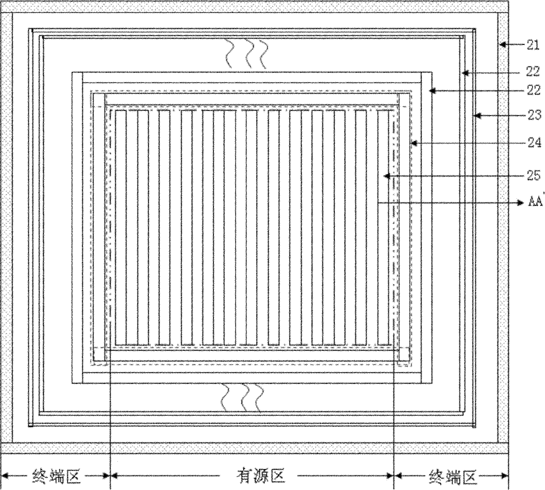
[0037] Embodiment two, such as Figure 6 As shown, the difference between the present embodiment and the first embodiment is that the shape of the annular groove 23 and the annular groove 22 in the structure of the terminal area is improved, and the four corners in the first embodiment are improved to be right-angled. The arc shape with a certain radian can further reduce the electric field intensity at the corner and increase the breakdown voltage of the device. In this embodiment, the four corners of the P-shaped ring 24 are also changed into circular arcs with a certain radian.

[0038] Implementation three, such as Figure 7 Shown, based on the plan view of embodiment one and embodiment two (see image 3 , 6 ), the position of the polysilicon field plate 8' is improved, and a polysilicon field is covered above the junction of each P / N thin layer (that is, the junction of the P-type semiconductor thin layer and the N-type semiconductor thin layer) outside the terminal re...

Embodiment 5

[0040] Embodiment five, such as Figure 9 As shown, on the basis of the third embodiment, all the field plates in the terminal area are changed to metal field plates, that is, the polysilicon field plate 8' located above the gate oxide film 7 is canceled, and the interlayer dielectric film 9 outside the terminal area A metal field plate 13' is provided at the junction of each P / N thin layer above.


PUM


Abstract

The invention discloses a terminal protection structure of a super-junction semiconductor device, which comprises a protective ring, field plates, a trench cut-off ring and a charge balance compensation P-type trench ring positioned in the trench cut-off ring, wherein the charge balance compensation P-type trench ring is provided with at least two types of trenches with different depths. The invention also discloses a fabrication method for the super-junction semiconductor device. Without increasing the complexity of the process, the invention can enhance the voltage-withstanding characteristic and reliability of the device.

Description

technical field [0001] The invention relates to the field of semiconductor integrated circuits, in particular to a terminal protection structure of a super junction semiconductor device. The invention also relates to a manufacturing method of the super junction semiconductor device. Background technique [0002] Super junction MOSFET (Metal Oxide Semiconductor Field Effect Transistor) adopts a new voltage-resistant layer structure, using a series of alternately arranged P-type and N-type semiconductor thin layers (or called semiconductor column layers), in the off state and lower voltage The P-type region and the N-type region are depleted to achieve mutual compensation of charges, so that the P-type region and the N-type region can achieve high breakdown voltage under high doping concentration, thereby obtaining low on-resistance and high breakdown at the same time voltage, breaking the theoretical limit of traditional power MOSFETs. Like the existing DMOS (Double Diffuse...

Claims


Application Information

Patent Timeline
Patent Type & Authority Patents(China)
IPC IPC(8): H01L29/06H01L29/78H01L21/336
Inventor 肖胜安韩峰
Owner SHANGHAI HUAHONG GRACE SEMICON MFG CORP
Why Eureka
Try Eureka