Semiconductor structure and manufacturing method thereof

A semiconductor and conductive pad technology, which is applied in semiconductor/solid-state device manufacturing, semiconductor devices, semiconductor/solid-state device components, etc. The problem of large bending degree of wire can achieve the effect of avoiding offset and dumping, avoiding oxidation or corrosion, and alleviating bending arc.

Active Publication Date: 2021-10-19
CHANGXIN MEMORY TECH INC
View PDF10 Cites 0 Cited by
  • Summary
  • Abstract
  • Description
  • Claims
  • Application Information

AI Technical Summary

Problems solved by technology

[0003] However, with the improvement of package integration, the distance between the I / O terminal of the chip and the package pin or the pad on the substrate is further reduced, because the I / O terminal of the chip is higher than the package pin or the pad on the substrate. , when the wire forms the first bonding point on the I / O terminal of the chip and the second bonding point on the package pin or the pad of the substrate, the height difference between the first bonding point and the second bonding point is relatively small Large and the distance between the first bonding point and the second bonding point is small, so that the bending degree of the metal wire is relatively large, and the first bonding point and the second bonding point are easy to crack, which affects the stability of the semiconductor structure

Method used


Image

  • Semiconductor structure and manufacturing method thereof
  • Semiconductor structure and manufacturing method thereof
  • Semiconductor structure and manufacturing method thereof

Examples


Embodiment Construction

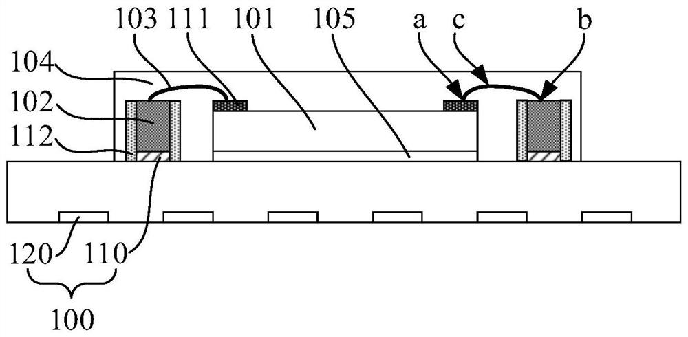
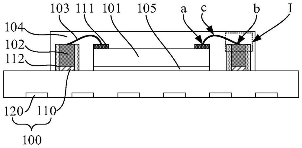
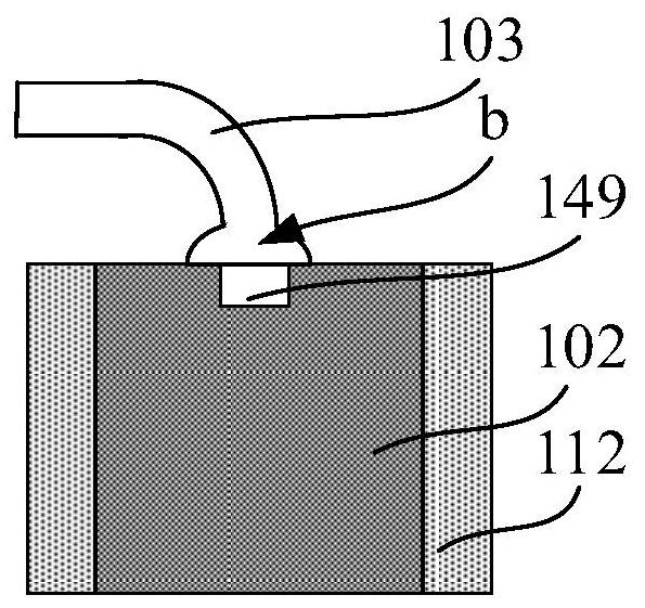
[0014] It can be seen from the background art that the current connection strength between the lead wire and the I / O terminal of the chip and the package pin or the pad on the substrate needs to be improved, and the stability of the semiconductor structure needs to be improved.

[0015] After analysis, it is found that in order to pursue higher packaging integration, the distance between the I / O terminal of the chip and the package pin or the pad on the substrate will inevitably be further reduced. At this time, the height difference between the I / O terminal of the chip and the package pin or the pad on the substrate will further increase the bending of the lead connecting the I / O terminal of the chip and the package pin or the pad on the substrate. The degree makes it easier for the lead to crack due to excessive bending at the I / O end of the chip and the package pin or the pad on the substrate.

[0016] In order to solve the above problems, the present invention provides a s...


PUM


Abstract

The embodiment of the invention provides a semiconductor structure and a manufacturing method thereof. The semiconductor structure comprises a substrate, a bonding pad which is disposed on the substrate and whose surface is exposed out of the substrate, a bonding column which is located on the surface, away from the substrate, of the bonding pad and makes contact with the bonding pad; a first device which is located on the substrate and spaced apart from the bonding column, a welding pad which is located on the surface of the first device away from the substrate, a lead which connects the bonding pad and the bonding column, and a protective dielectric layer which extends along the side wall of the bonding column. According to the embodiment of the invention, the connection strength between the lead and the bonding column and the bonding pad is improved, and the protection effect on the bonding column is enhanced, so that the stability of the semiconductor structure is improved.

Description

technical field [0001] Embodiments of the present invention relate to the field of semiconductors, and in particular to a semiconductor structure and a manufacturing method thereof. Background technique [0002] With the advancement of technology, the degree of integration and integration of semiconductor packaging is gradually enhanced, and electronic equipment is developing in the direction of miniaturization, high speed, high reliability, low cost and low power consumption. Connections in semiconductor packages are usually made by wire bonding. Wire bonding (Wire Bonding) is to use wires to interconnect the I / O terminals of the chip with the corresponding package pins or pads on the substrate. In the solid-phase welding process, heating, pressure and ultrasonic energy are used to destroy the surface oxide layer and pollution, produce plastic deformation, and electron sharing and atomic diffusion occur in the intimate contact of the interface to form solder joints. [00...

Claims


Application Information

Patent Timeline
Patent Type & Authority Applications(China)
IPC IPC(8): H01L23/498H01L21/48H01L21/60
CPCH01L23/49811H01L23/49838H01L24/48H01L21/4853H01L24/85H01L2224/48091H01L2224/48229
Inventor 张丽霞刘杰应战
Owner CHANGXIN MEMORY TECH INC
Why Eureka
Try Eureka