
Silicon-based power device structure based on substrate bias technology

A technology for power devices and substrates, applied in semiconductor devices, electrical components, circuits, etc., can solve the problems of small safe working area, difficult manufacturing process, and low reliability.

Inactive Publication Date: 2012-04-11
GUILIN UNIV OF ELECTRONIC TECH
View PDF0 Cites 15 Cited by
  • Summary
  • Abstract
  • Description
  • Claims
  • Application Information

AI Technical Summary

Problems solved by technology

However, SOI-based power devices inevitably bring about the problems of difficult manufacturing process, high cost, small safe operating area and low reliability. The structure of silicon-based power devices based on substrate bias technology has not been reported yet.

Method used


Image

  • Silicon-based power device structure based on substrate bias technology
  • Silicon-based power device structure based on substrate bias technology
  • Silicon-based power device structure based on substrate bias technology

Examples


Embodiment Construction

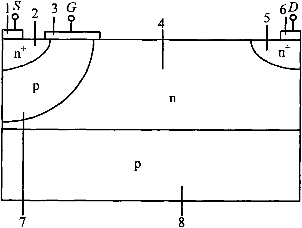
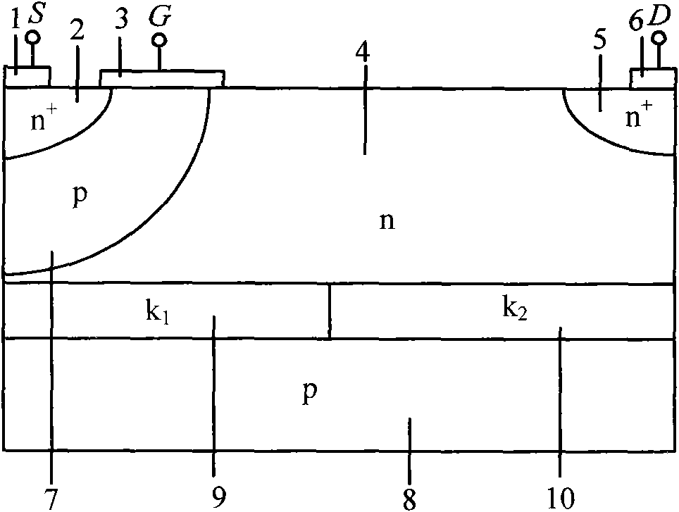
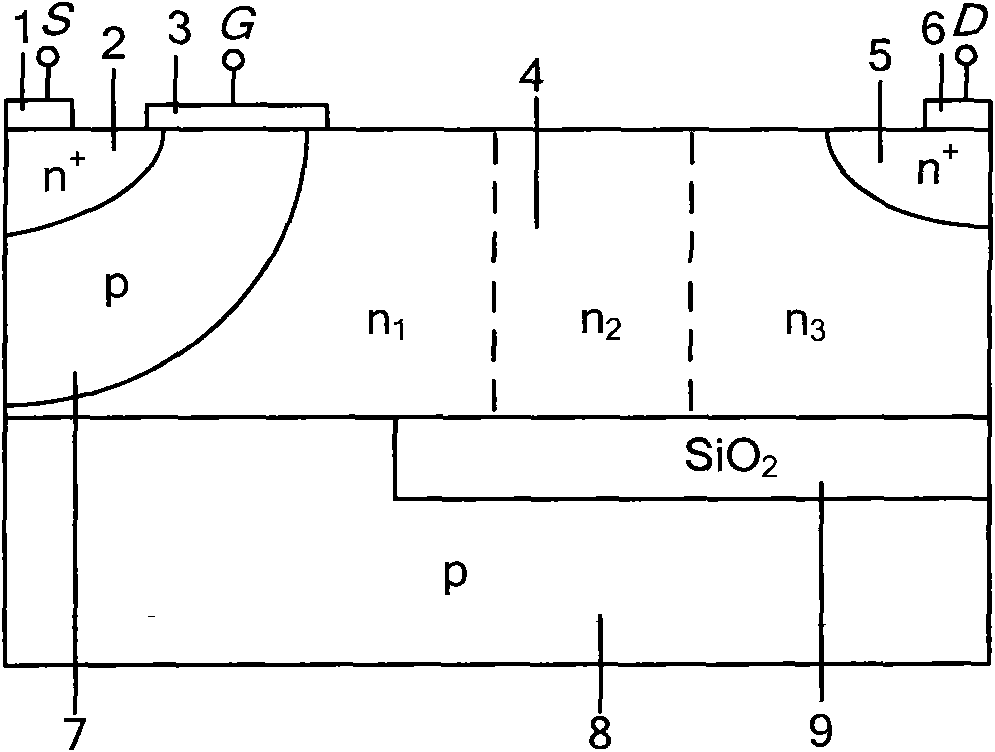
[0045] By adopting the silicon-based power device structure based on the substrate bias technology of the present invention, a power device with high breakdown voltage and low conduction loss with excellent performance can be obtained, especially a high-voltage silicon-based power device of 600V-1200V can be realized. The silicon-based high-voltage device structure based on the substrate bias technology provided by the present invention includes a buried layer silicon-based power device structure based on the substrate bias technology ( Figure 6 and Figure 7 ), D-RESURF silicon-based power device structure based on substrate bias technology ( Figure 8 ) and variable doped silicon-based power device structure based on substrate bias technology ( Figure 9 ). The silicon-based device structure based on substrate bias technology can be combined with surface termination technology to form a variety of device structures. These termination technologies and structures are field ...


PUM


Abstract

The invention belongs to the technical field of semiconductor power devices. A silicon-based power device based on a substrate bias technology forms a reverse-biased PN junction by a compound substrate structure with reverse conduction type; by the electric field distribution in a substrate electric-field modulator, the longitudinal electric-field peak value is reduced, and the whole blocking voltage born by the conventional power device in the longitudinal direction is changed into a part of the blocking voltage, so that the voltage resistance of the device is enhanced, and the compromise relation of the power device between conducting resistance and breakdown voltage is improved. By utilization of the silicon-based substrate bias technology provided by the invention, the structure of the device can be designed by flexibly combining multiple surface terminal technologies. The silicon-based power device structure can be utilized for manufacturing various high-voltage-resistant devices with excellent performance, for example, the power devices such as lateral double-diffusion field effect transistors, PN diodes and lateral insulated gate bipolar type power transistors and the like.

Description

technical field [0001] A silicon-based power device structure based on substrate bias technology belongs to the technical field of semiconductor power devices, and in particular relates to the technical field of silicon-based power device withstand voltage. Background technique [0002] An ideal power device should have ideal static and dynamic characteristics, be able to withstand high voltage in the off state, and have large current and low voltage drop in the on state. The lateral device electrodes are all on the surface of the chip, which is easy to realize integration with low-voltage signal circuits through internal connections, and the driving circuit is simple. As a commonly used lateral power device, LDMOS (lateral double diffused MOS) has the advantages of thermal stability against secondary breakdown, less localized current concentration, fast switching speed and good frequency characteristics. [0003] The structure of a typical conventional n-type LDMOS is as ...

Claims


Application Information

Patent Timeline
Patent Type & Authority Applications(China)
IPC IPC(8): H01L29/78H01L29/06
Inventor 李琦左园
Owner GUILIN UNIV OF ELECTRONIC TECH
Learn More