
Power amplifier with adjustable output power

A power amplifier and output power technology, applied in power amplifiers, impedance networks, electrical components, etc., can solve the problems of high implementation cost, complex implementation structure, large area, etc., to improve efficiency, improve reverse isolation and stability. Effect

Active Publication Date: 2014-05-28
UNIV OF SCI & TECH OF CHINA
View PDF6 Cites 0 Cited by
  • Summary
  • Abstract
  • Description
  • Claims
  • Application Information

AI Technical Summary

Problems solved by technology

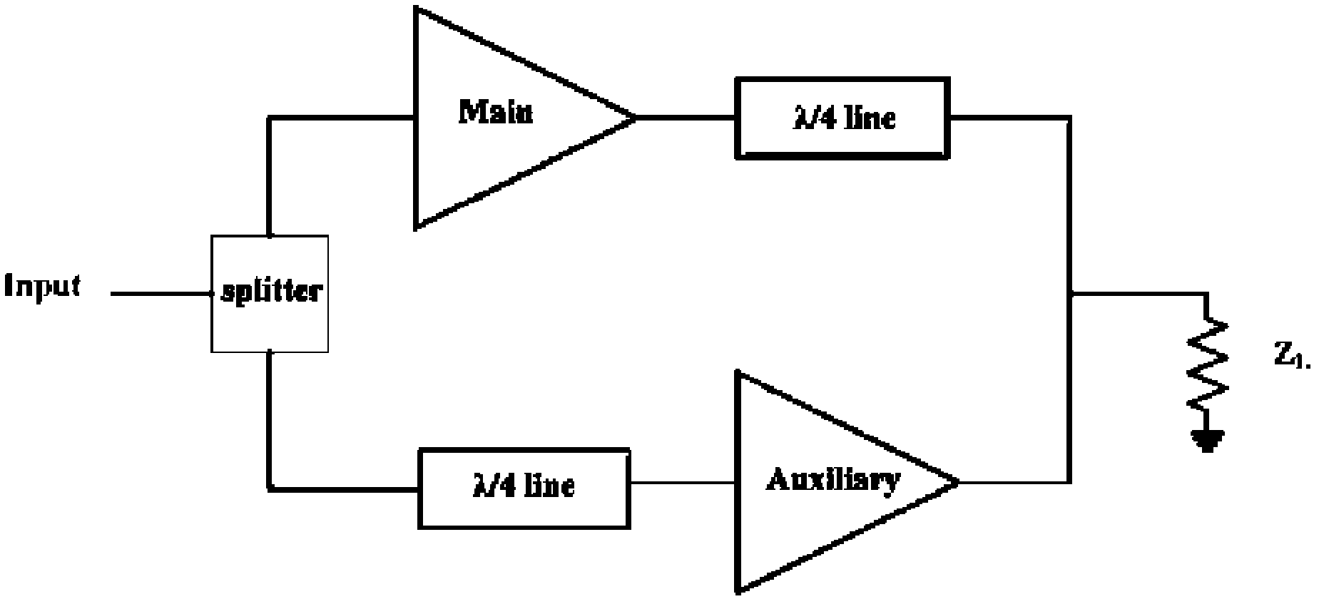
In the working range of 1GHz to 10Ghz, the length of the quarter-wavelength transmission line is tens of millimeters or even tens of centimeters, which is too expensive or even unrealistic to realize in the integrated circuit process
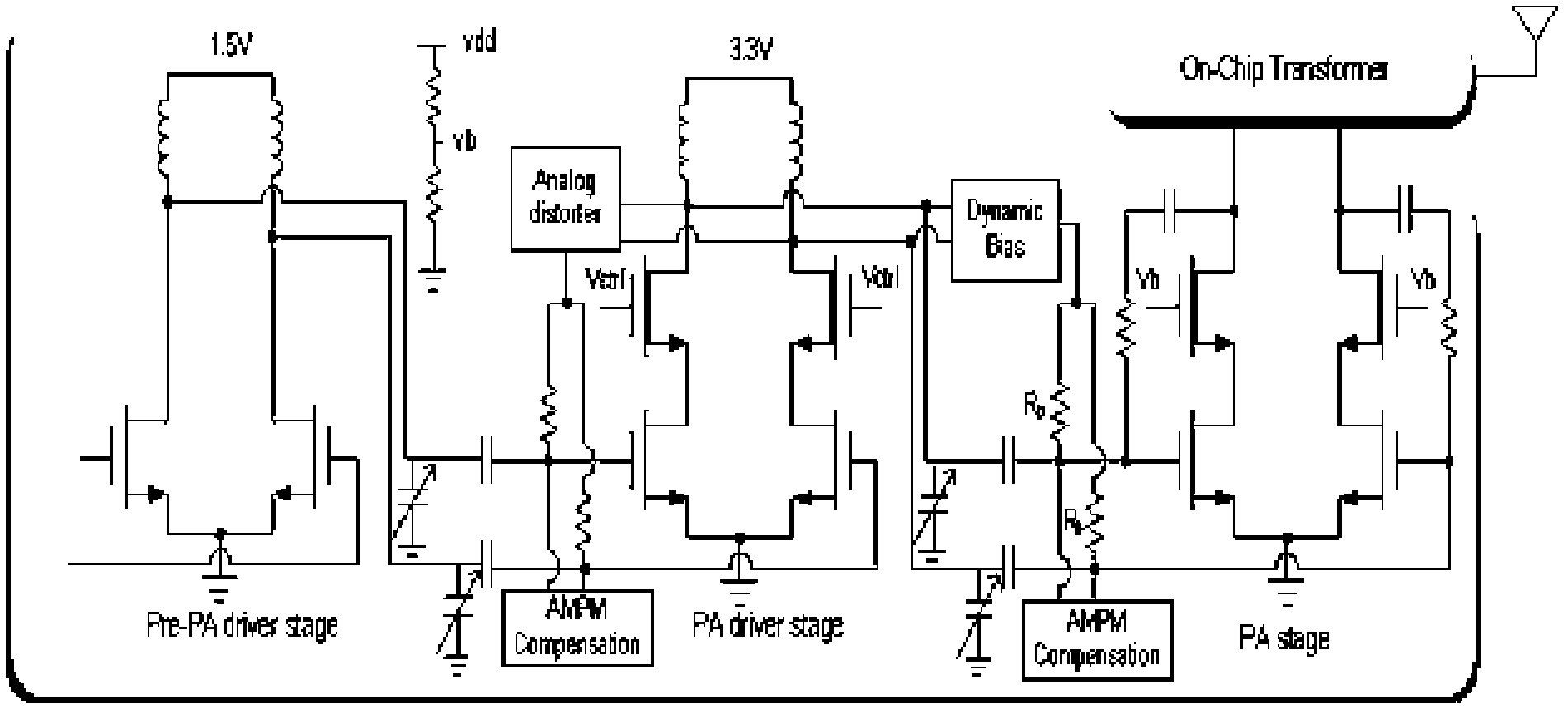
Therefore, literature [3] uses discrete components to realize the transmission line, but as Figure 4 As shown, the implementation structure is complicated, multiple inductors are used, the layout area is large, and the cost is high
[0007] Now there are many patents related to the impedance transformation network. For example, the patent application number 200610164854.9 proposes a matching network. Capacitor, two inductors, the area is too large
In addition, such as the patent application number 200980113014.1, the disclosed network single-ended circuit needs four capacitors and four inductors, which also has the problem of too large area.

Method used


Image

  • Power amplifier with adjustable output power
  • Power amplifier with adjustable output power
  • Power amplifier with adjustable output power

Examples


Embodiment 1

[0040] Figure 7 Shows Figure 6 A specific implementation of the main power amplifier 1. In the figure, only two sub-power amplifiers are connected in parallel, that is, the power sub-amplifier 13 and the sub-power amplifier 14 are connected in parallel, but it is obvious that the parallel connection of multiple sub-power amplifiers also belongs to the application of the present invention.

[0041] For the power sub-amplifier 13, the source terminals of the transistor NM1 and the transistor NM2 are grounded, the gate terminal is connected with the switch control signal SW1, the drain terminals of the transistor NM1 and the transistor NM2 are connected, and are connected with the source terminals of the transistor NM5 and the transistor NM6, forming a Switch to ground for one of the sub-amplifiers. The purpose of connecting the drain terminals of the transistor NM1 and the transistor NM2 is to realize a virtual ground on the circuit and increase the gain. Transistor NM5, th...

Embodiment 2

[0047] Figure 8 Shows Figure 6 A specific implementation of the matching network circuit 2. Specifically, a structure of a differential capacitor variable matching network is shown, and a switched capacitor array is used to realize impedance transformation. Obviously, the variable capacitance matching network can be easily applied to single-ended circuits, which also belongs to the scope of the present invention. There are many ways to realize the switch, and a very simple way is to use an NMOS tube to realize it. In this embodiment, four switched capacitor arrays are used for the impedance conversion rate adjustment capacitor, and two switched capacitor arrays are used for the resonant frequency adjustment capacitor. Obviously, other numbers of capacitor arrays can be used according to actual applications to achieve the required tuning range and accuracy.

[0048] Two parallel switch arrays (C8, SW5 are connected in series to form one capacitor array, C9, SW6 are connect...

Embodiment 3

[0051] Figure 9 Shows Figure 6 A specific overall implementation of the embodiment, in order to further illustrate this embodiment 3, will Figure 7 and Figure 8 put together to form Figure 9 , the output end of Embodiment 1 is connected in series with the input end of Embodiment 2, that is, Embodiment 3 is realized. When the switches SW5, SW6, SW7, and SW8 are all turned on, the impedance conversion rate adjustment capacitance is the largest, and the impedance conversion rate is the lowest at this time, and the equivalent resistance seen at the output end of the main power amplifier is the smallest. At this time, the switch control signal of the main power amplifier SW1 and SW2 are turned on, and the sub-power amplifier 1 and sub-power amplifier 2 included in the main power amplifier work together to achieve the maximum output power. When the switches SW5, SW6, SW7, and SW8 are all disconnected, the impedance conversion rate mediation capacitance is the smallest, and ...


PUM


Abstract

The invention provides a power amplifier with an adjustable output power, which comprises a main power amplifier (1) and a matching network circuit (2). The output end of the main power amplifier (1) is connected with the input end of the matching network circuit (2). The switch control power amplifier and a neutralizing capacitor technique are adopted, and the two ends of one switch array (11) of the main power amplifier (1) are respectively connected between the ground and the power amplifier; and the two ends of the other switch array (12) of the main power amplifier (1) are respectively connected between a power supply and the power amplifier, the switch control power amplifier is enabled to be better compatible with the neutralizing capacitor technique and the reverse isolation degree and the stability are improved. Besides, since the matching network circuit (2) with variable capacitors is adopted, by adjusting capacitors (6 and 7), the impedance conversion rate can be adjusted and a capacitor (5) is adjusted at the same time to enable the circuit resonance frequency to reach set frequency. The power amplifier with adjustable output power can meet the need of multi-power output in the existing power transmitting technique, the stability and the reverse isolation degree of the multi-power output are improved and the efficiency during power back-off is improved.

Description

technical field [0001] The invention belongs to the technical field of radio frequency integrated circuits, and specifically relates to a power amplifier with adjustable output power. The power amplifier can be applied to various wireless communication systems. The circuit structure of the power amplifier in the invention is suitable for CMOS, BiCMOS, FET, Mass junction transistors and other transistors. Background technique [0002] In various wireless transmission technologies, due to different actual environments, such as distances, obstacles, and interferences, power amplifiers are often required to provide different output powers to meet the compromise between low power consumption and actual needs, and if each network The nodes can dynamically adjust the output power, which will greatly reduce the background noise of the communication environment. In fact, many communication products have power fallback function, such as TI's zigbee chip cc2530, the maximum output pow...

Claims


Application Information

Patent Timeline
Patent Type & Authority Patents(China)
IPC IPC(8): H03F3/20H03H7/01
Inventor 贾非林福江刁盛锡
Owner UNIV OF SCI & TECH OF CHINA
Learn More