Sectional type through hole modeling method including influence of plane on resonance characteristic

A technology of resonance characteristics and modeling methods, applied in special data processing applications, instruments, electrical digital data processing, etc., can solve problems such as large computer resources, long calculation time, and unfavorable design optimization.

Active Publication Date: 2013-11-13
BEIHANG UNIV
View PDF2 Cites 0 Cited by
  • Summary
  • Abstract
  • Description
  • Claims
  • Application Information

AI Technical Summary

Problems solved by technology

Method (1) is suitable for low-frequency occasions, and the research is relatively mature, and it is no longer a research hotspot at present; method (2) uses FEM, FDTD, TML and other methods for modeling to study the characteristics of vias, and the simulation results are more accurate. However, the calculation method takes a long time and takes up a lot of computer resources, which is not conducive to the optimization of the design. Therefore, methods (3) and (4) are currently research hotspots.

Method used


Image

  • Sectional type through hole modeling method including influence of plane on resonance characteristic
  • Sectional type through hole modeling method including influence of plane on resonance characteristic
  • Sectional type through hole modeling method including influence of plane on resonance characteristic

Examples


Embodiment 1

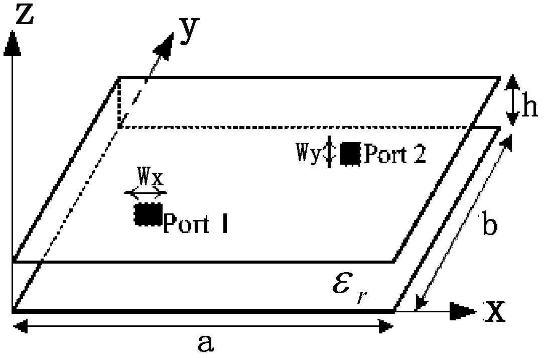
[0144] The size of the PCB board is: length a=1600mil, width b=1400mil, including three plane pairs, the thickness from top to bottom is: d1=10mil, d2=63.3mil, d3=10mil, the microstrip line and the adjacent The distance between the plates is h=5.7mil. The size of the via hole is: hole radius r viabody =6mil, pad radius r of the hole pad = 10mil, the anti-pad radius of the hole is r antipad = 20mil. The line width of the microstrip is w=10mil, and the length L=25mil. The material of the plate is metal copper, the thickness is t=1mil, and the dielectric constant ε is adopted as the medium r = 4.4 for FR4 material.

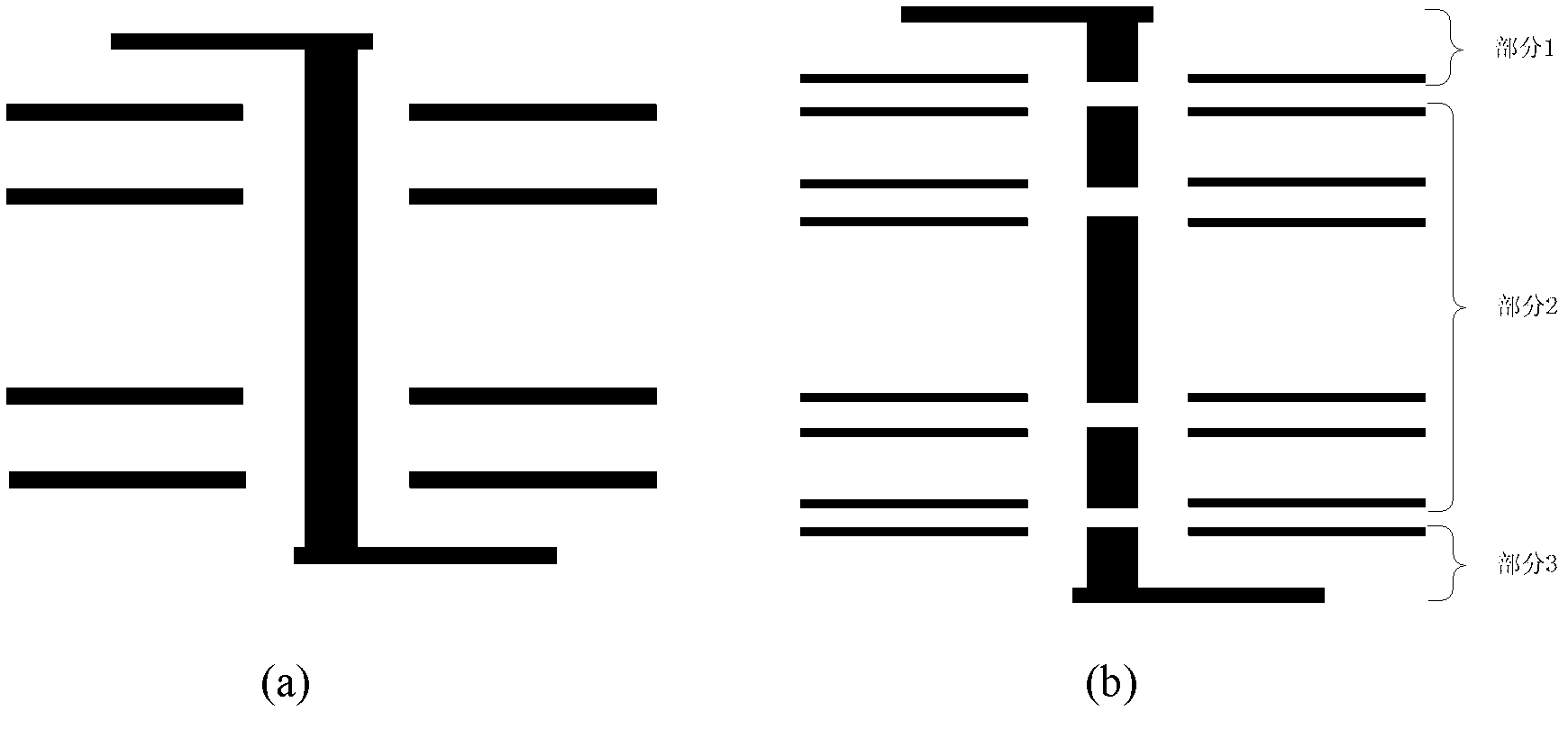
[0145] (1) Single via

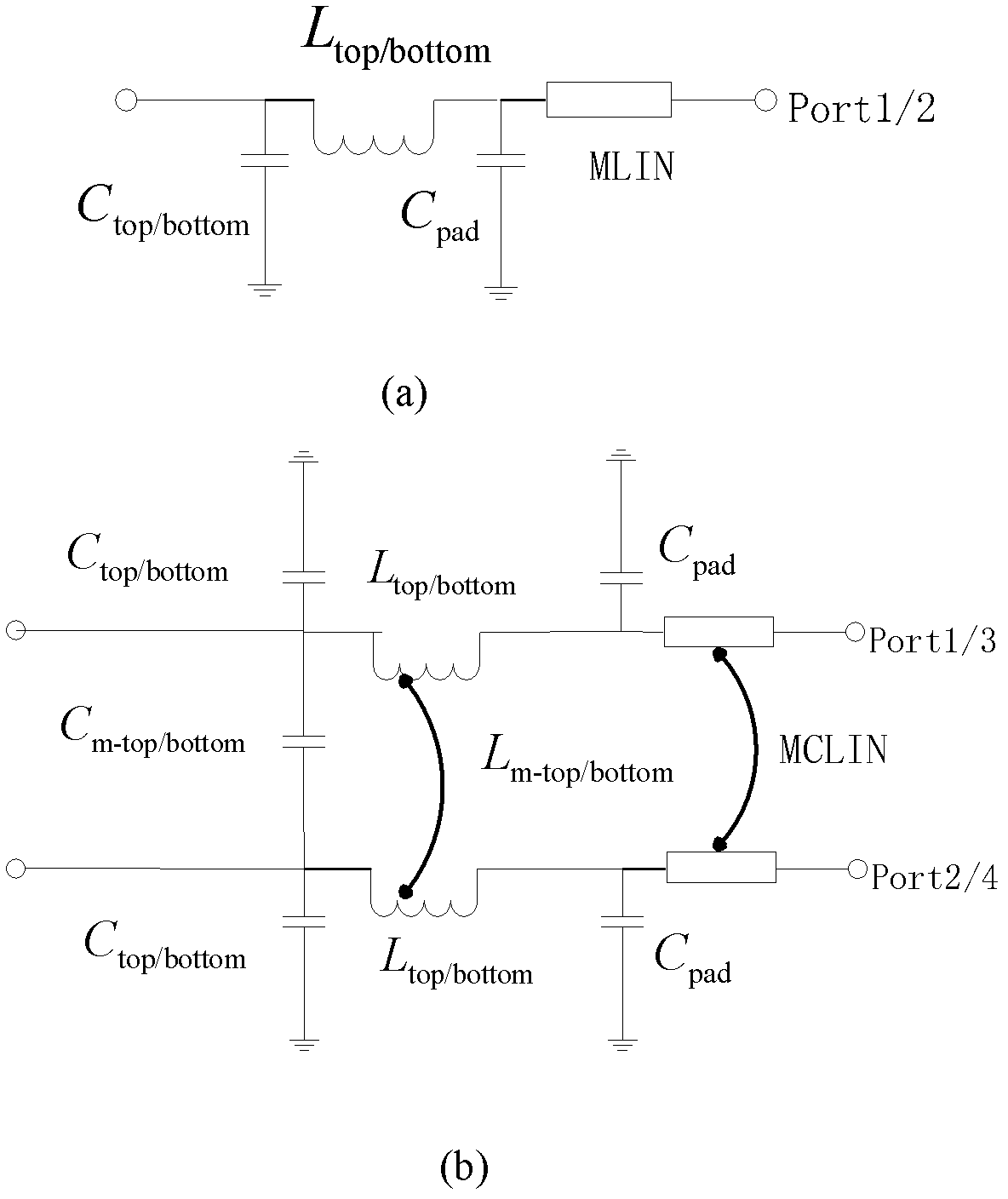
[0146] Step 1: Decompose the via structure at the center of each plate, and divide it into the vertical conversion structure from the top microstrip line to the upper part of the via, the middle vertical via structure 1, the middle vertical via structure 2, and the middle vertical via structure. The hole structure 3 and the lower part o...


PUM


Abstract

The invention discloses a sectional type through hole modeling method including influence of a plane on a resonance characteristic. The type through hole modeling method comprising the seven steps of: 1, decomposing a through hole structure in a center position of each flat plate; 2, extracting capacitor and inductor parameters in all parts of equivalent circuits of a through hole; 3, building an equivalent circuit map of a top microstrip line to an upper through hole vertical conversion structure and a lower through hole to a bottom microstrip line vertical conversion structure; 4, extracting a parameter impedance of the plane to a position where the center of a circle of the through hole is; 5, adding a Zpp obtained in the step 4 to an equivalent circuit model of an intermediate vertical through hole; 6, sequentially cascading all equivalent circuits of the through hole according to the upper part, the middle part and the lower part, and respectively adding a terminal port at two ends of the final equivalent circuit; and 7, building a one-order circuit model with a through hole structure in an ADS (Application Development System), establishing a physical model of the through hole in a simulation software HFSS (High Frequency Structure Simulator), calculating an S11 parameter and an S21 parameter, and comparing the obtained result with the result in the step 6.

Description

(1) Technical field [0001] The invention relates to a segmented via-hole modeling method including the influence of the plane on resonance characteristics, which is a modeling method of a typical interconnection structure on a printed circuit board - a via-hole, and its essence is to decompose and construct the via-hole structure Each section is modeled as a second-order inductance-capacitance equivalent circuit, and the influence of the resonant characteristics of the plane pair on the transmission characteristics of the via is considered during the modeling process, and finally the equivalent circuit of each part of the via is cascaded modeling method. This method is simple, fast and accurate. It belongs to the field of board-level electromagnetic compatibility modeling and simulation of electronic engineering. (2) Background technology [0002] The topology of the circuit on the printed circuit board is complex, and there are a large number of components and high-freque...

Claims


Application Information

Patent Timeline
Patent Type & Authority Patents(China)
IPC IPC(8): G06F17/50
Inventor 阎照文车明明韩雅静于文璐
Owner BEIHANG UNIV
Why Eureka
Try Eureka