
Block power tube circuit and mtehod for realizing same
A technology of power tube and block, which is applied in the direction of programmable logic circuit device, output power conversion device, logic circuit connection/interface layout, etc., can solve the problems of deteriorating output ripple and limited improvement of efficiency, etc., and achieve the reduction of conduction pass loss, improve efficiency, and reduce loss
- Summary
- Abstract
- Description
- Claims
- Application Information
AI Technical Summary
Problems solved by technology
Method used
Image

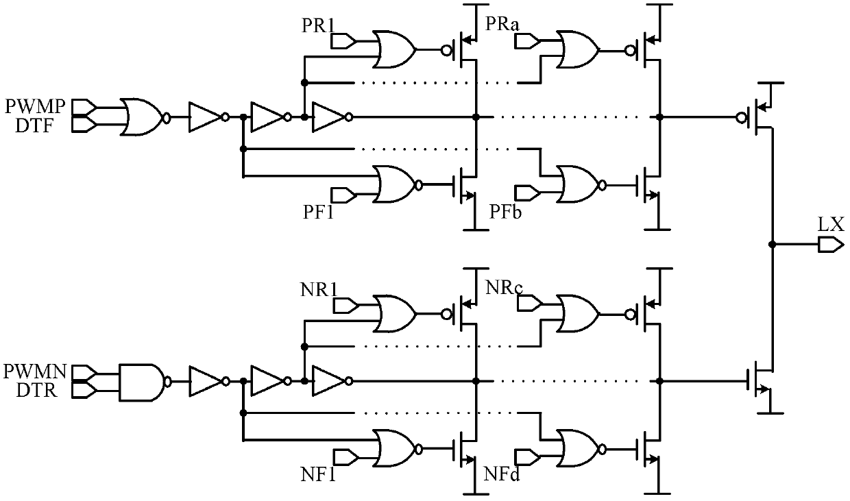
Examples
Embodiment 1
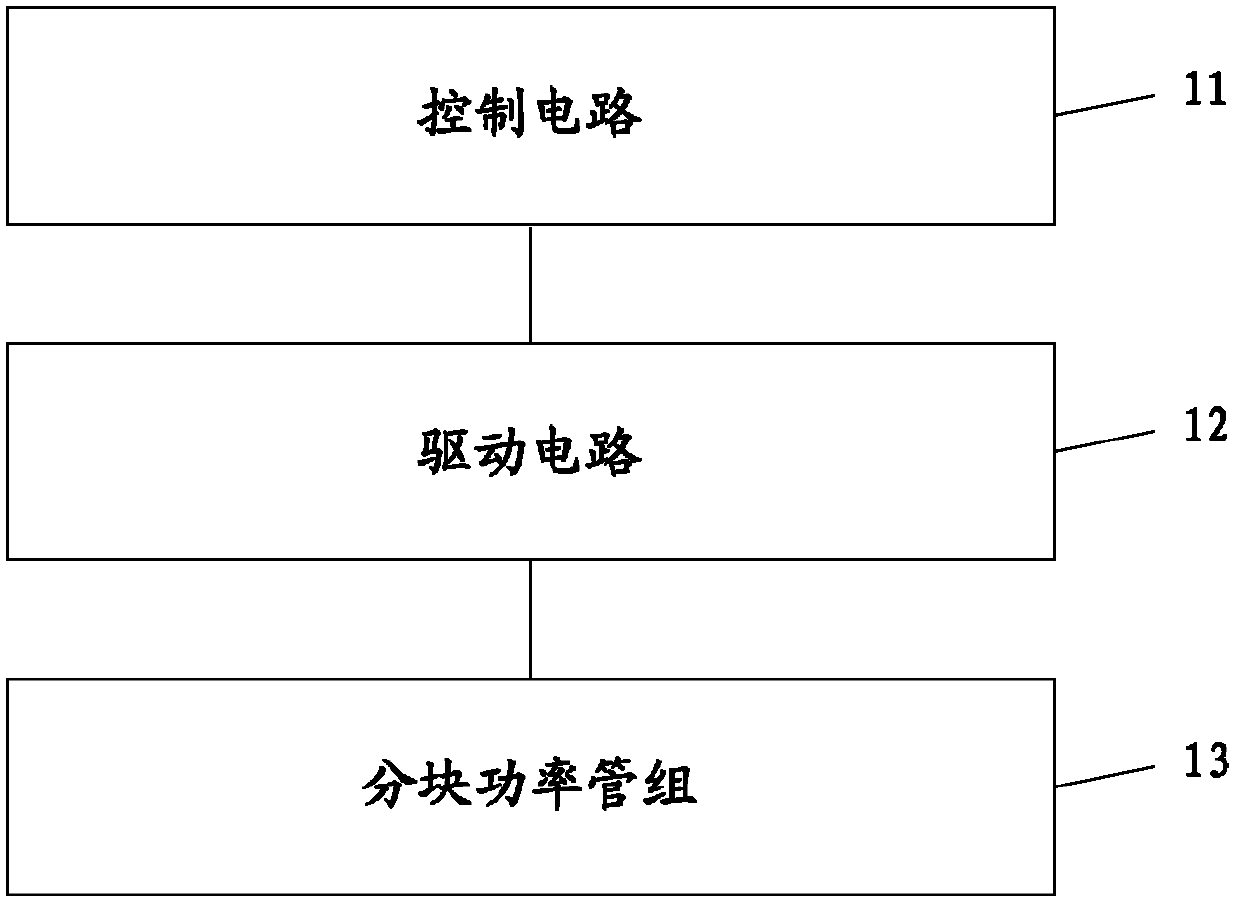
[0026] This embodiment provides a block power tube circuit, which is used to logically control the voltage adjustment signal of the switching power supply, so as to realize the power supply voltage required by the processor and memory connected to the switching power supply, and manage the power supply voltage in the current switching power supply. The switching state of the power tube, such as figure 1 As shown, the circuit includes a control circuit 11, a drive circuit 12 and a block power tube group 13, wherein:
[0027] The control circuit 11 is used to adjust the square-wave duty ratio of the PWM signal according to the voltage adjustment signal, generate a PWMP signal, a PWMN signal and a control signal m, and the control signal m is used to manage the number of power tube pairs turned on and then adjust the switch The efficiency of the power supply, the PWMP signal and the PWMN signal are used to provide the power tube state control signal for the drive circuit 12, wher...
Embodiment 2
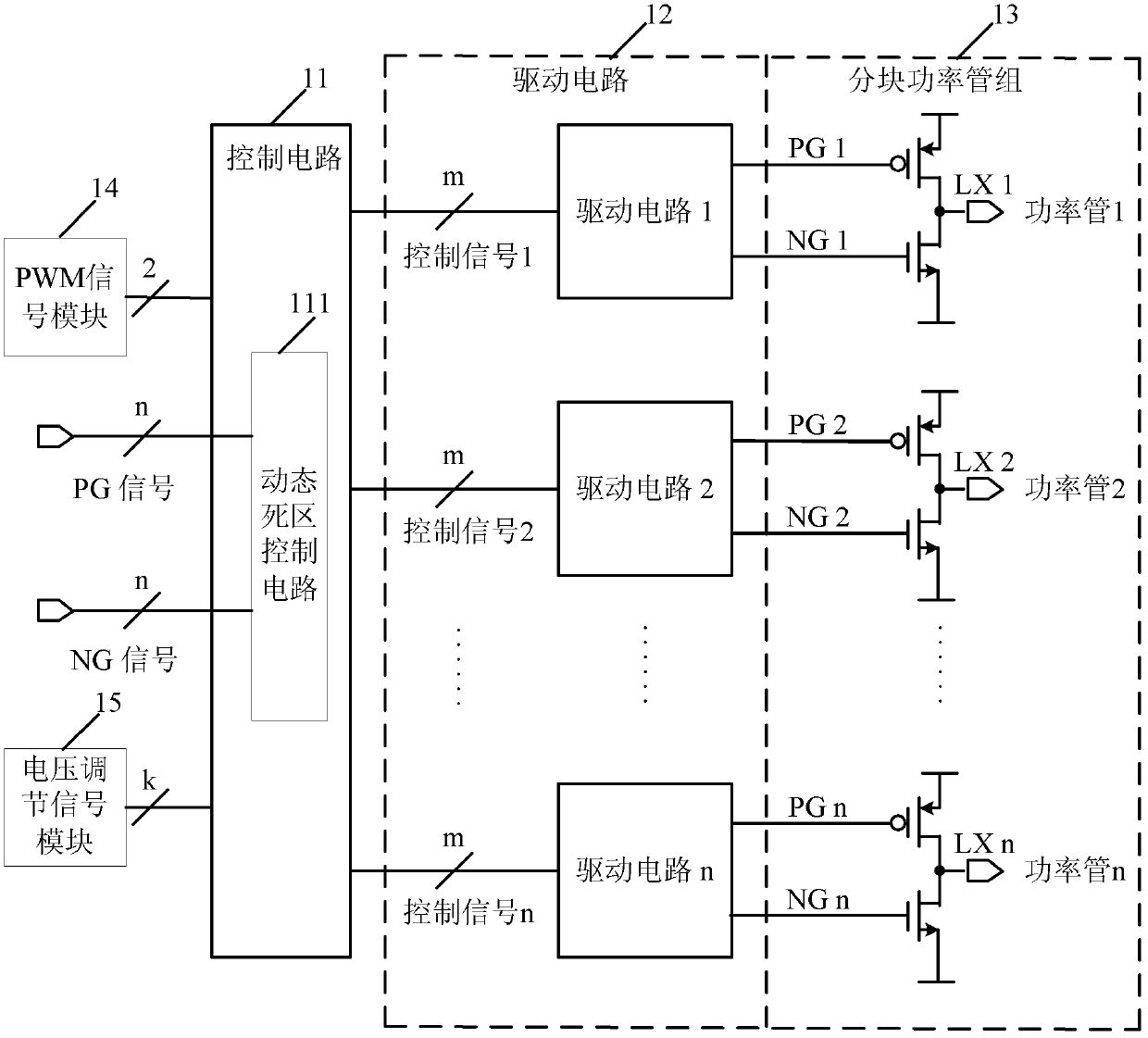
[0032] This embodiment provides a block power tube circuit, which is used to logically control the voltage adjustment signal of the switching power supply, so as to realize the power supply voltage required by the processor and memory connected to the switching power supply, and manage the power supply voltage in the current switching power supply. The switching state of the power tube, such as figure 2 As shown, the circuit includes a control circuit 11, a drive circuit 12 and a block power tube group 13, wherein:
[0033]The control circuit 11 is used to adjust the square-wave duty ratio of the PWM signal according to the voltage adjustment signal, generate a PWMP signal, a PWMN signal and a control signal m, and the control signal m is used to manage the number of power tube pairs turned on and then adjust the switch The efficiency of the power supply, the PWMP signal and the PWMN signal are used to provide the power tube state control signal for the drive circuit 12, wher...
Embodiment 3
[0053] This embodiment provides a method for implementing a block power tube circuit, such as Image 6 As shown, the method includes:
[0054] 601. Generate a voltage adjustment signal according to the power supply voltage required by the processor and memory connected to the switching power supply, use the PWM signal and the voltage adjustment signal to generate a PWMN signal, a PWMP signal, and a control signal m through the control circuit, and pass The control signal m manages the number of power transistor pairs turned on.
[0055] 602. The PWMP signal and the PWMN signal generate drive signals PG and NG through the drive circuit, and the PG signal controls the switching state of the PMOS power transistor in the power transistor pair, and the NG signal controls the switching state of the NMOS power transistor in the power transistor pair.
[0056] Further, the block power tube circuit also includes a dynamic dead zone control circuit, and the method further includes:
...
PUM
 Abstract
Description
Claims
Application Information