Polishing pad, polyurethane layer therefor, and method of polishing a silicon wafer

A polyurethane layer, polishing pad technology, applied in the field of 20 to 200 micron pores, chemical-mechanical polishing pads, can solve problems such as increased surface roughness, undulation damage, chemical properties of CMP pads and mechanical structure deterioration

Inactive Publication Date: 2012-05-09
ROGERS CORP
View PDF48 Cites 20 Cited by
  • Summary
  • Abstract
  • Description
  • Claims
  • Application Information

AI Technical Summary

Problems solved by technology

[0007] In addition, when using highly active polishing compositions to polish semiconductor wafers, the chemical properties and mechanical structure of the CMP pad may be degraded
As a result, the efficiency of the polis...

Method used


Image

  • Polishing pad, polyurethane layer therefor, and method of polishing a silicon wafer
  • Polishing pad, polyurethane layer therefor, and method of polishing a silicon wafer
  • Polishing pad, polyurethane layer therefor, and method of polishing a silicon wafer

Examples


Embodiment 1

[0123] Polyurethane layers were prepared by the method described above using the formulations shown in Table 3.

[0124] table 3

[0125] Example 1

components

number of copies

Part A

PTMEG

60.60

MP diol

13.70

triol

13.41

Surfactant

1.88

Catalyst-1

5.81

PTFE No.2

4.61

Total, Part A

100.01

OH#

284

Part B

Isocyanate

94.46

total number of copies

[0126] Materials prepared according to this formulation are rigid microcellular high modulus polyurethanes. For Example 1, the M of the foamed cured polyurethane C (Molecular weight between crosslinking points) is equal to 4521.33.

[0127] To test the material for CMP polishing, a polishing pad made from the formulation of Example 1 (Example P-1) was used for copper planarization, which was then compared to a conventional IC1000 CMP pad made by Rohm and Haas . T...

Embodiment 2

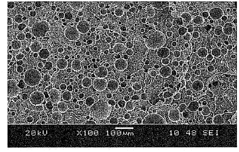
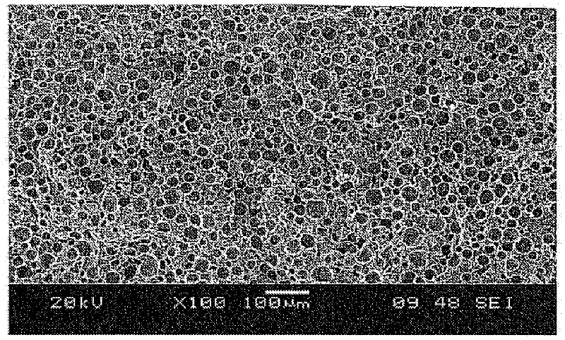
[0141] Different formulations containing hydrophobic particles were prepared. figure 1 shows a scanning electron microscope (SEM) of a polyurethane material prepared generally according to the examples described herein without the use of PTFE microparticles, figure 2 A comparable formulation using PTFE microparticles is shown. The effect of the PTFE microparticles in the polyurethane foam was to produce smaller and more consistent cells based on the SEM images.

[0142] Measured using the above surface energy test figure 2 The surface of the polyurethane material in the surface. The results of contact angle (CA) and surface energy are shown in Table 6.

[0143] Table 6

[0144]

[0145] Therefore, it is believed that the presence of hydrophobic particles reduces the surface energy of the polyurethane material. In forming a CMP polishing pad, the resulting surface can be abraded, which can change the measured surface energy of the polyurethane.

Embodiment 3-6

[0147] These examples illustrate the tuning of the modulus properties of polyurethane materials for CMP polishing by varying the concentrations of the individual components of the reaction mixture used to form the polyurethane materials. Top pads based on the two formulations shown in Table 7 were prepared.

[0148] Table 7

[0149] Example 3

Example 4

Material

number of copies

number of copies

Part A

PTMEG polyol

66.41

63.41

MP diol

7.89

10.89

triol

13.41

13.41

Surfactant

3.76

3.76

Catalyst-2 *

5.81

5.81

PTFE No. 2

4.61

4.61

Total Copies, Part A

101.89

101.89

OH#

280

315

Part B

Isocyanate

93.01

106.65

[0150] * dilute with polyol

[0151] The microporous topsheet prepared according to Example 3 was similar to the formulation of Example 1 above...


PUM

PropertyMeasurementUnit
Densityaaaaaaaaaa
Median particle sizeaaaaaaaaaa

Abstract

A polyurethane layer for forming a polishing pad for a semiconductor wafer is described, wherein the polyurethane layer comprises: a foamed polyurethane, wherein the polyurethane foam has a density of about 640 to about 960 kg/m3, and a plurality of cells having an average diameter of about 20 to about 200 micrometers; and particles of a hydrophobic polymer having a critical surface energy of less than 35 mN/m and having a median particle size of 3 to 100 micrometers. Polishing pads as well as methods for polishing are also described.

Description

Background technique [0001] The present application relates to articles and methods for chemical-mechanical polishing. In particular, the present invention relates to chemical-mechanical polishing pads for precise and rapid polishing of semiconductor wafer surfaces and the like. [0002] In recent years, chemical-mechanical polishing (CMP) has become the technology of choice for semiconductor chip manufacturers to planarize the surface of semiconductor chips when laying circuit pattern layers. CMP techniques are well known and are commonly accomplished with polishing pads and polishing compositions. [0003] The fabrication of semiconductor wafers typically involves the formation of multiple integrated circuits on a semiconductor substrate such as silicon, gallium arsenide, indium phosphide, or the like. The integrated circuits are typically formed by a series of process steps in which patterned layers of materials such as conductive, insulating and semiconducting materials ...

Claims


Application Information

Patent Timeline
IPC IPC(8): B24B37/14B24D13/14
CPCC08G18/222C08L75/04B24B37/24C08G18/10C08L27/18C08G2101/0066B24B37/22B24B37/26C08G2110/0066C08G18/6607C08L2666/04B24B37/04B24D13/14H01L21/304
Inventor 布赖恩·利特克迈克尔·K·科斯
Owner ROGERS CORP
Why Eureka
Try Eureka