Manufacturing method of mosfet and mosfet
A manufacturing method and source region technology, which is applied in semiconductor/solid-state device manufacturing, electrical components, circuits, etc., can solve problems such as gate oxide layer gate oxide breakdown, so as to improve service life and reduce the possibility of breakdown , the effect of increasing the thickness
- Summary
- Abstract
- Description
- Claims
- Application Information
AI Technical Summary
Problems solved by technology
Method used
Image
Examples
Embodiment 1
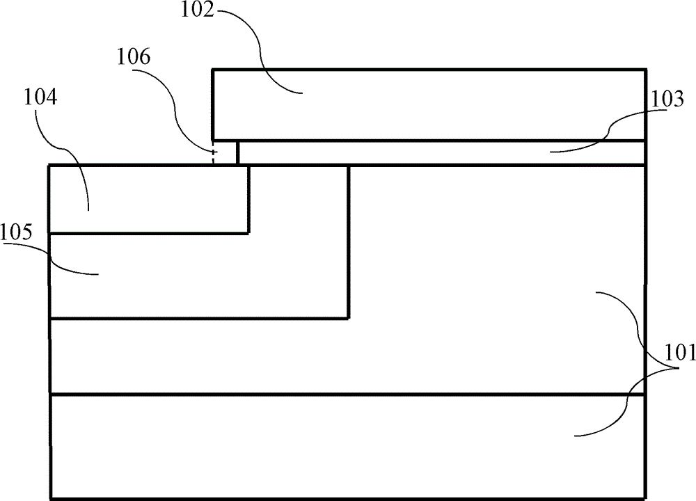
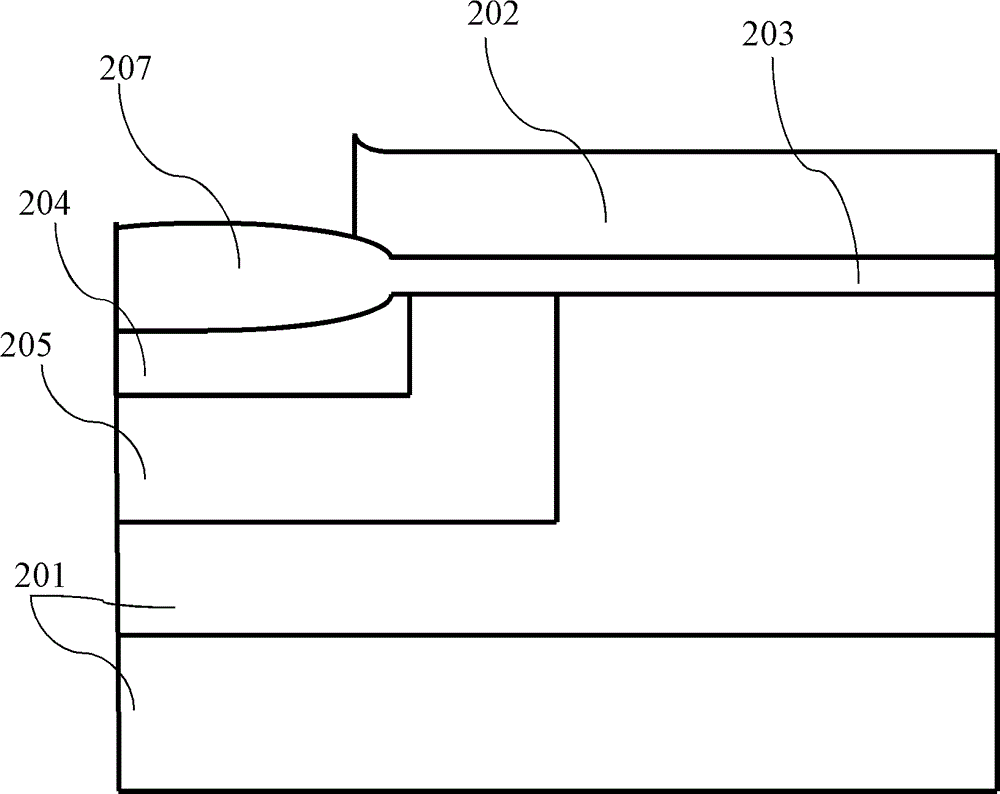
[0049] This embodiment provides a method for manufacturing a MOSFET. After the source region is formed and before the dielectric layer is formed, the method includes:
[0050] forming a gate oxide layer and a polysilicon gate on the surface of the epitaxial layer;
[0051] forming a source region within the surface of the epitaxial layer;
[0052] Oxidation of the source region is performed to form an oxide on the surface of the source region in the space between the polysilicon gate and the source region.
[0053] It should be noted that the epitaxial layer in this embodiment can be N - ~N + type structure, the thickness of the epitaxial layer can be determined according to the specific application requirements of the device, and the epitaxial layer can be located on the front or back of the semiconductor wafer.
[0054] In this step, the specific method for forming the gate oxide layer can be: using a thermal oxidation process to form a gate oxide layer on the surface of ...
Embodiment 2
[0062] This embodiment provides a specific MOSFET manufacturing method. On the basis of the method provided in Embodiment 1, in this embodiment, before the source region is formed, it may further include:
[0063] On both sides of the polysilicon gate, a body region is formed by ion implantation and impurity push well;
[0064] The source region is formed within the body region.
[0065] Using the polysilicon gate as a mask, ion implantation is performed on both sides of the polysilicon gate, and impurities are pushed into wells to form body regions. In a subsequent step, the source region is formed by implanting impurities in the body region.
[0066] In this embodiment, before forming the gate oxide layer and the polysilicon layer, a conductive protection region for protecting devices and implementing device isolation may also be formed in the semiconductor wafer, and the implementation may include:
[0067] forming an oxide protection layer on the surface of the epitaxial...
Embodiment 3
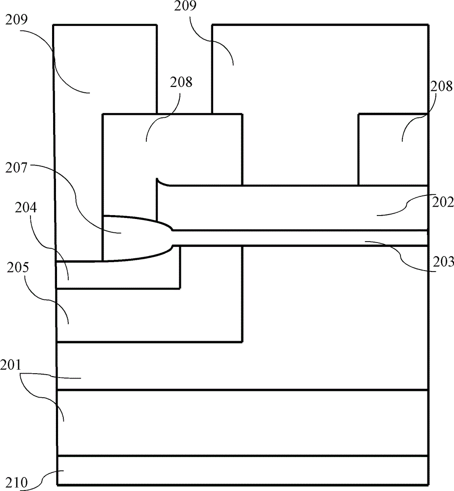
[0085] Corresponding to the foregoing method embodiments, this embodiment further provides a MOSFET.
[0086] The MOSFET includes an epitaxial layer, a source region formed in the surface of the epitaxial layer, a gate oxide layer and a polysilicon gate formed on the surface of the epitaxial layer;
[0087] On the surface of the source region of the MOSFET, in the gap between the polysilicon gate and the source region, an oxide layer formed by a thermal oxidation growth process is arranged.
[0088] Preferably, the thickness of the oxide layer may be 1-3 times the thickness of the gate oxide layer.
[0089] Since this embodiment obtains the device structure embodiment by applying the above method embodiment, the similarities thereof can be referred to each other, and will not be repeated here.
[0090] In the embodiment of the present invention, the oxide formed on the surface of the source region fills the gap between the edge of the polysilicon gate and the source region, a...
PUM
 Abstract
Description
Claims
Application Information
 - R&D
- Intellectual Property
- Life Sciences
- Materials
- Tech Scout
- Unparalleled Data Quality
- Higher Quality Content
- 60% Fewer Hallucinations
Browse by: Latest US Patents, China's latest patents, Technical Efficacy Thesaurus, Application Domain, Technology Topic, Popular Technical Reports.
© 2025 PatSnap. All rights reserved.Legal|Privacy policy|Modern Slavery Act Transparency Statement|Sitemap|About US| Contact US: help@patsnap.com


