Supercharge Your Innovation With Domain-Expert AI Agents!

Trench isolation structure and forming method for same

一种沟槽隔离、沟槽的技术,应用在半导体器件、电气元件、电路等方向,能够解决漏电流、影响半导体器件性能等问题,达到改善性能、结合紧密、减小尺寸的效果

Active Publication Date: 2012-05-30
INST OF MICROELECTRONICS CHINESE ACAD OF SCI
View PDF4 Cites 3 Cited by
  • Summary
  • Abstract
  • Description
  • Claims
  • Application Information

AI Technical Summary

Problems solved by technology

However, due to the influence of subsequent steps such as the planarization process and the cleaning process after planarization, in the shallow trench isolation structure of the prior art, there will be an orientation between the surface of the dielectric layer 11 and the surface of the adjacent semiconductor substrate 10 . The lower recessed area is called the side ditch (Divot) 12, and the side ditch is easy to cause problems such as leakage current, which affects the performance of semiconductor devices.

Method used


Image

  • Trench isolation structure and forming method for same
  • Trench isolation structure and forming method for same
  • Trench isolation structure and forming method for same

Examples


Embodiment Construction

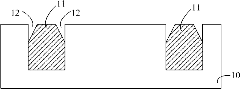
[0047] In the shallow trench isolation structure formed in the prior art, side trenches exist between the surface of the dielectric layer filled in the shallow trench and the surface of the semiconductor substrate, which will generate leakage current and affect the performance of the semiconductor device.

[0048] In the shallow trench isolation structure of the prior art, the material used for the dielectric layer is an amorphous material, such as silicon oxide, silicon nitride, etc. The inventors have found through research that since the material of the semiconductor substrate is a crystalline material, the amorphous material The combination between the dielectric layer and the semiconductor substrate of the crystalline material is not tight enough, so that it is easy to generate side grooves at the junction of the amorphous material and the crystalline material during the planarization and subsequent cleaning processes, resulting in leakage current and affecting the performa...


PUM


Abstract

Disclosed are a trench isolation structure and a forming method for the same. The trench isolation structure comprises a semiconductor substrate and trenches formed on the surface of the semiconductor substrate, and dielectric layers made of crystal materials are filled in the trenches. By the aid of the trench isolation structure, the sizes of side trenches can be reduced, and the performance of a semiconductor device is improved.

Description

technical field [0001] The invention relates to the field of semiconductor manufacturing, in particular to a trench isolation structure and a forming method thereof. Background technique [0002] As the semiconductor technology enters the deep submicron era, shallow trench isolation structures (STI) are mostly used for isolation between active areas of semiconductor devices such as implanted MOS transistors. The specific formation process mainly includes: forming a shallow trench on the semiconductor substrate by etching and other processes, and the shallow trench is used to isolate the active region on the semiconductor substrate; after that, filling the shallow trench with a dielectric material, The dielectric material fills the shallow trench and covers the surface of the semiconductor substrate; finally, the dielectric material is planarized until the surface of the semiconductor substrate is exposed, and the method of planarization may be chemical mechanical polishing....

Claims


Application Information

Patent Timeline
Patent Type & Authority Applications(China)
IPC IPC(8): H01L21/762H01L29/78
CPCH01L21/76224H01L29/02H01L21/76232
Inventor 钟汇才赵超梁擎擎
Owner INST OF MICROELECTRONICS CHINESE ACAD OF SCI
Features
  • R&D
  • Intellectual Property
  • Life Sciences
  • Materials
  • Tech Scout
  • Unparalleled Data Quality
  • Higher Quality Content
  • 60% Fewer Hallucinations
Learn More