Novel fine metal mask plate for producing organic light emitting diode (OLED) display panel and fabrication method of novel fine metal mask plate

一种精细金属掩膜、显示面板的技术,应用在金属材料涂层工艺、图纹面的照相制版工艺、离子注入镀覆等方向,能够解决图像单元损坏、成本昂贵等问题,达到降低制作成本、增加强度、简化制作过程的效果

Active Publication Date: 2013-12-18
ZHONGSHAN XINNUO MICROELECTRONICS CO LTD
View PDF2 Cites 46 Cited by
  • Summary
  • Abstract
  • Description
  • Claims
  • Application Information

AI Technical Summary

Problems solved by technology

[0005] In addition, due to the manufacturing process of OLED, it is necessary to prevent the pattern in the fine metal mask from defects caused by residual substances by cleaning every once in a while, which can easily cause damage to some image units in the fine metal mask, so Fine metal masks must be replaced approximately every two months
Due to the above factors, the cost of fine metal masks in the production process of OLED display panels is quite expensive

Method used


Image

  • Novel fine metal mask plate for producing organic light emitting diode (OLED) display panel and fabrication method of novel fine metal mask plate
  • Novel fine metal mask plate for producing organic light emitting diode (OLED) display panel and fabrication method of novel fine metal mask plate
  • Novel fine metal mask plate for producing organic light emitting diode (OLED) display panel and fabrication method of novel fine metal mask plate

Examples


Embodiment Construction

[0055] The present invention is described in detail below in conjunction with accompanying drawing:

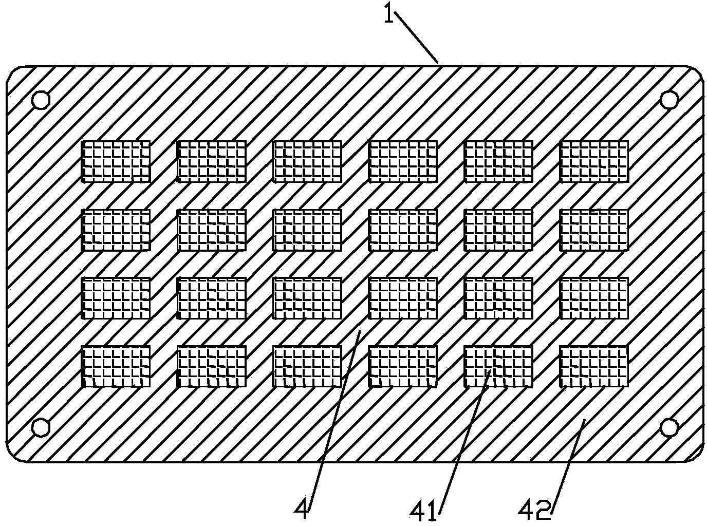
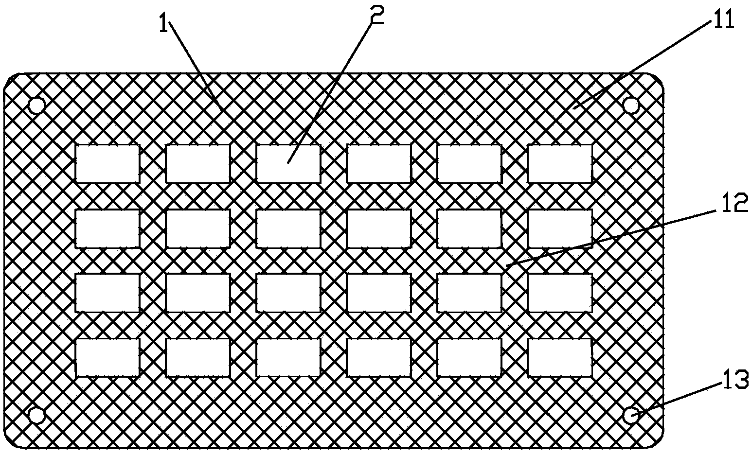
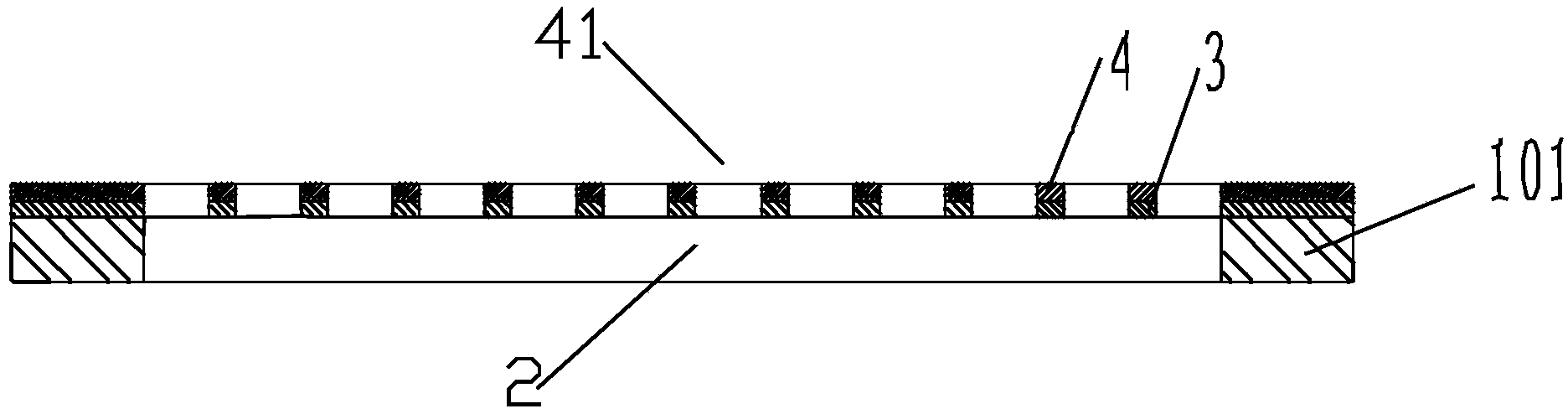
[0056] Such as figure 1 , figure 2 As shown, a new type of fine metal mask plate for OLED display panel production includes a frame 1 composed of an outer frame 11 and an inner partition frame 12, and the frame 1 is formed by setting a plurality of through holes 2 on a metal substrate . A fine mask 4 is electroformed on the frame 1, so that the fine mask 4 and the frame 1 are integrated. The fine mask 4 is divided into two parts: a graphic area (fine structure part) 41 and a frame area 42, and an alignment hole 13 for positioning the mask plate is also provided on the outer frame 11 of the frame 1, and the number of alignment holes is two or more than two, there are four here. The graphic area 41 has the same area and corresponding position as the through hole 2 on the frame.

[0057] Such as Figure 3-Figure 15 As shown, a sectional view of a through hole 2 and its sur...


PUM


Abstract

The invention discloses a novel fine metal mask plate for producing an organic light emitting diode (OLED) display panel and a fabrication method of the novel fine metal mask plate. The novel fine metal mask plate comprises a border formed by a plurality of through holes formed in a metal substrate, wherein a layer of fine mask is electroformed on the upper surface of the border, so that the fine mask and the border are combined into a whole; the fine mask divides a pattern area and a border area, on which a part with a fine structure is formed; the through holes in the pattern area and the border correspond to each other. The fabrication method comprises the following steps: A, preparing the metal substrate, namely carrying out rough shape cutting on an invar alloy plate or a stainless steel plate, so as to accord with the design size and form the metal substrate; B, fabricating the fine mask, namely coating a photoresist layer on the metal substrate, developing required patterns on the photoresist layer on the metal substrate, and orderly electroforming a metal substrate layer and a metal layer with a low coefficient of thermal expansion, so as to form the fine mask of the mask plate; and C, etching the substrate, namely dividing the pattern area on the refine mask, etching off the metal substrate in a district corresponding to the back part of the pattern area by a chemical etching method, so as to form the through holes, and leaving an external border and an internal partition frame, so that the external border and the internal partition frame jointly support the fine mask.

Description

【Technical field】 [0001] The invention relates to the technical field of semiconductor manufacturing, and more specifically relates to a novel fine metal mask for OLED display panel production and a manufacturing method. 【Background technique】 [0002] The current production of OLED (organic light-emitting diode, also known as organic laser display, which has self-luminous characteristics) display panels with high pixel density requires the use of fine metal masks (Fine Metal Mask, FMM) with very thin thickness and small thermal expansion coefficient. ) as a mask (or shadow mask) for evaporating the organic luminous body (three primary colors) in the pixel of the OLED panel. [0003] The fine metal mask plate for OLED is usually prepared by chemical etching using Invar alloy (INVAR, also known as Invar). First, photoresist or photosensitive dry film is coated on the surface of Invar alloy, and the The fine pattern of the mask plate is transferred on the photosensitive film,...

Claims


Application Information

Patent Timeline
Patent Type & Authority Applications(China)
IPC IPC(8): C23C14/04
CPCC23C14/042C23F1/02C23F1/04G03F7/0015G03F7/00
Inventor 杜卫冲韩建崴梅文辉
Owner ZHONGSHAN XINNUO MICROELECTRONICS CO LTD
Why Eureka
Try Eureka