Circuit board and manufacturing method thereof

A technology of circuit boards and circuit substrates, applied in multilayer circuit manufacturing, printed circuit components, secondary treatment of printed circuits, etc., can solve the problems of copper surface oxidation, not longer, moisture absorption of insulating material layer, etc., and achieve weather resistance Good, low surface energy effect

Active Publication Date: 2012-05-30
QING DING PRECISION ELECTRONICS HUAIAN CO LTD +1
View PDF3 Cites 5 Cited by
  • Summary
  • Abstract
  • Description
  • Claims
  • Application Information

AI Technical Summary

Problems solved by technology

However, during the storage process of the existing circuit boards, there are problems such as possible oxidation of the copper surface and possible moisture absorption of the insulating material layer.
Even if the copper surface is protected by methods such as gold plating and immersion silver, the effective storage period is basically only about one year, not longer

Method used


Image

  • Circuit board and manufacturing method thereof
  • Circuit board and manufacturing method thereof
  • Circuit board and manufacturing method thereof

Examples


Embodiment Construction

[0066] The circuit board provided by the technical solution and its manufacturing method will be further described in detail below in conjunction with the accompanying drawings and multiple embodiments.

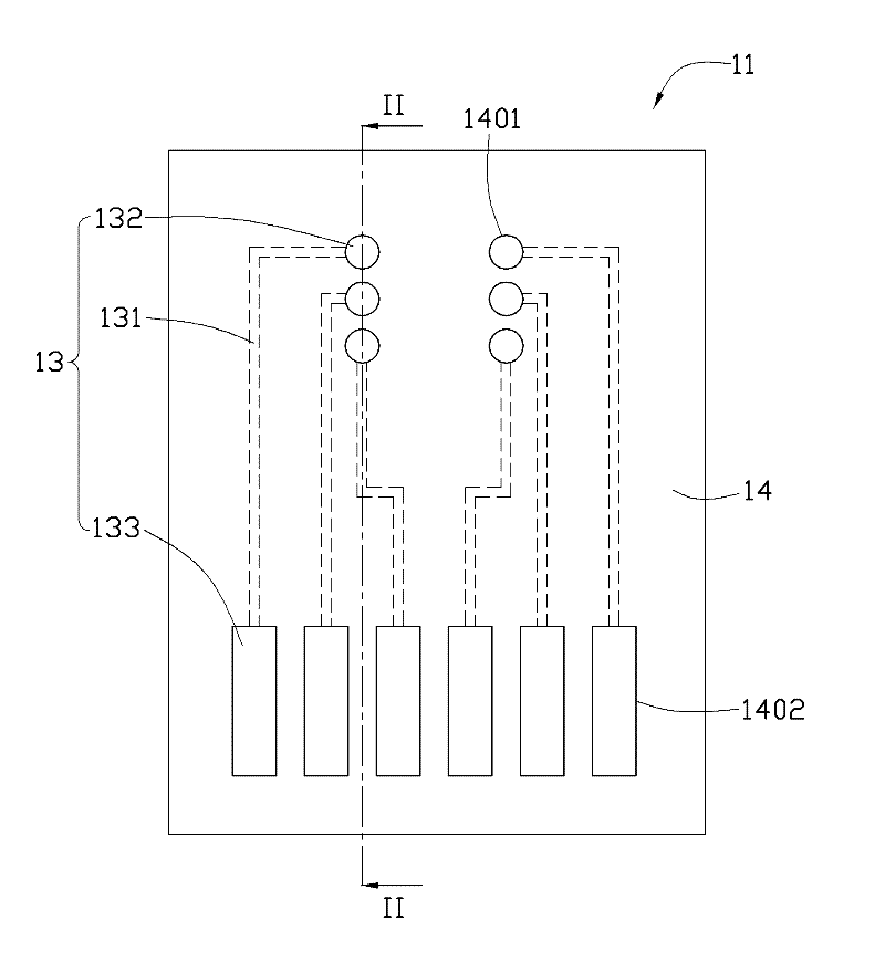
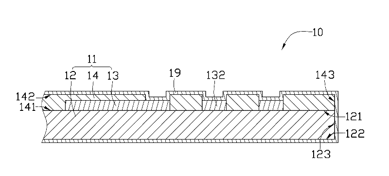
[0067] Please also refer to figure 1 and figure 2 , The circuit board 10 provided by the first embodiment of the technical solution includes a circuit substrate 11 and a fluorocarbon film 19 . The circuit substrate 11 includes a substrate 12 , a circuit layer 13 and a protection layer 14 stacked in sequence.

[0068] The base 12 can be a single-layer structure or a multi-layer structure. The single-layer structure refers to a structure including only one insulating layer. The multi-layer structure refers to a structure including at least one insulating layer and at least one conductive layer. The insulating layer can be a hard resin layer, such as epoxy resin, glass fiber cloth, etc., or a flexible resin layer, such as polyimide (Polyimide, PI), polyethylene terephthalat...


PUM


Abstract

The invention provides a circuit board which comprises: a substrate, a line layer, a protective layer and a fluorocarbon film. The substrate possesses a first surface. The line layer is formed on the first surface. The line layer comprises: a plurality of conductive lines and a plurality of conductive terminals. The protective layer covers the conductive lines and the first surface of the substrate which is exposed from the line layer. A first protective layer possesses a first protection surface which is close to the substrate and a second protection surface which is opposite to the first protection surface. The first protective layer is provided with a plurality of through holes which pass through the first protection surface and the second protection surface so as to expose the conductive terminals. The fluorocarbon film is deposited on the second protection surface and the surfaces of the conductive terminals. The fluorocarbon film is formed by carbon elements and fluoride elements and a ratio of a fluorine atom quantity to a quantity is 1.2 to 1.5. The circuit board of the invention has a long storage life. The technical scheme also provides a manufacturing method of the circuit board.

Description

technical field [0001] The invention relates to circuit board technology, in particular to a circuit board which can be stored for a long time and a manufacturing method thereof. Background technique [0002] With the advancement of science and technology, printed circuit boards are widely used in electronic products. For the application of the circuit board, please refer to the literature Takahashi, A.Ooki, N.Nagai, A.Akahoshi, H.Mukoh, A.Wajima, M.Res.Lab, High density multilayer printed circuit boardfor HITAC M-880, IEEE Trans. on Components, Packaging, and Manufacturing Technology, 1992, 15(4): 418-425. [0003] With the deepening of the protection of consumer rights and interests, suppliers of electronic products are required to provide maintenance parts for the entire service life of their products. According to the 10-year service life of general electronic products, it means that suppliers must keep product components for 10 years. However, during the storage proc...

Claims


Application Information

Patent Timeline
Patent Type & Authority Applications(China)
IPC IPC(8): H05K3/28H05K3/46H05K1/02
Inventor 白耀文
Owner QING DING PRECISION ELECTRONICS HUAIAN CO LTD
Why Eureka
Try Eureka