Metal deposition using seed layers

Inactive Publication Date: 2012-08-30
GMZ ENERGY +2
View PDF6 Cites 51 Cited by
  • Summary
  • Abstract
  • Description
  • Claims
  • Application Information

AI Technical Summary

Benefits of technology

[0016]The methods of the present invention, especially when metallic nanoparticles are used, can also be effective in selective metallization of portion of a substrate by selectively applying a seed layer to a portion of the surface and then preferentially depositing the electrically conducting metal on the selectively applied seed layer. For example, the seed layer can be selectively applied to a portion of the surface by employing photolithography, screen printing, inkjet printing, micro-contact stamping or dip-pen nanolithog

Problems solved by technology

However, these material property advances have not fully translated into better overall performance in the thermoelectric devices due at least in part to variations in the thermal and electrical contact resistances between the nanostructured alloy substrates and the metallized electrodes.
A poorly formed contact generates localized Joule heating effects and leads to a non-uniform current distribution which lowers an effective figure-of-merit (ZTeff) for the thermoelectric device from that of the thermoelectric material.
Direct electroplating on smooth, low-roughness, or hydrophobic surfaces of g

Method used


Image

  • Metal deposition using seed layers
  • Metal deposition using seed layers
  • Metal deposition using seed layers

Examples


Embodiment Construction

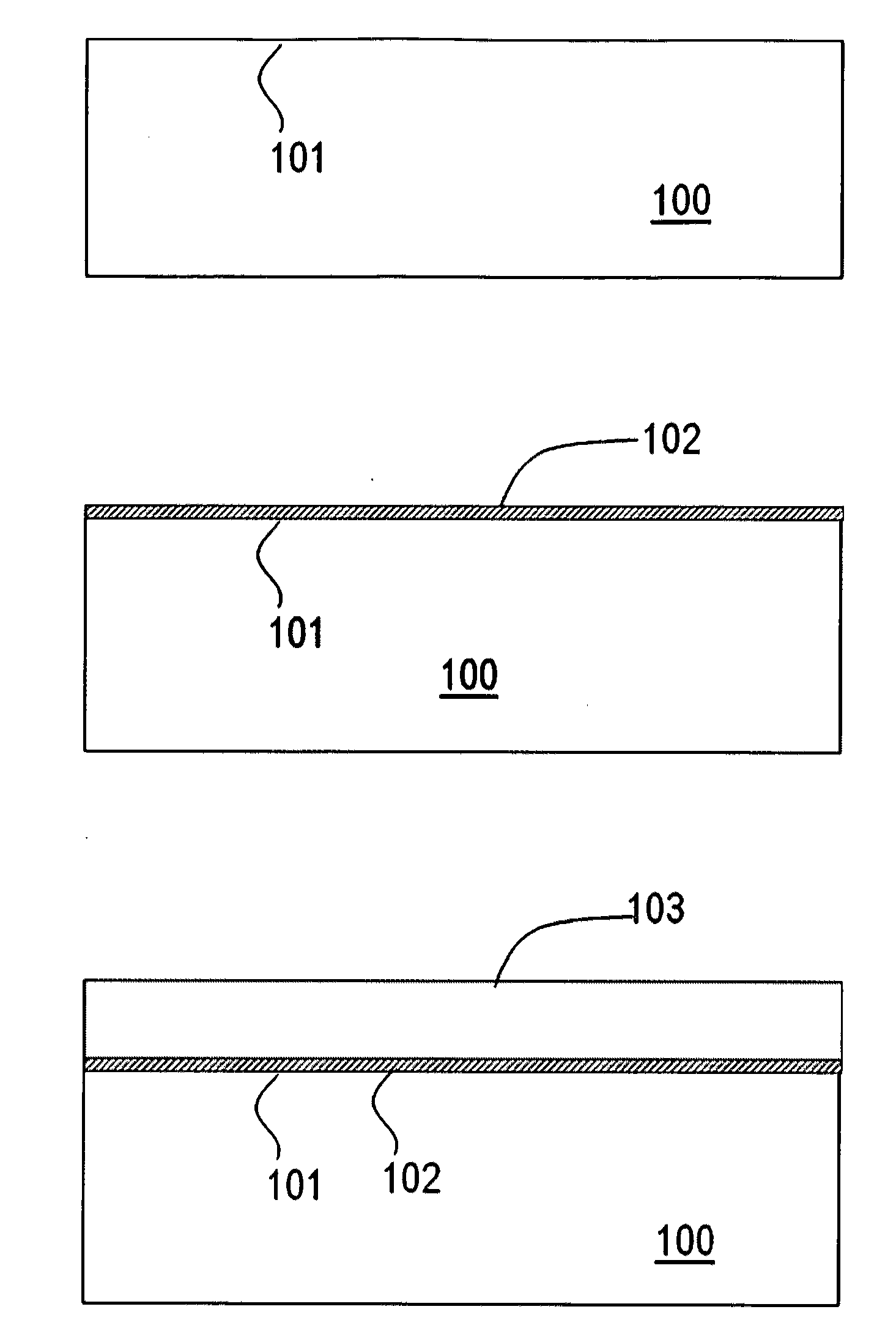
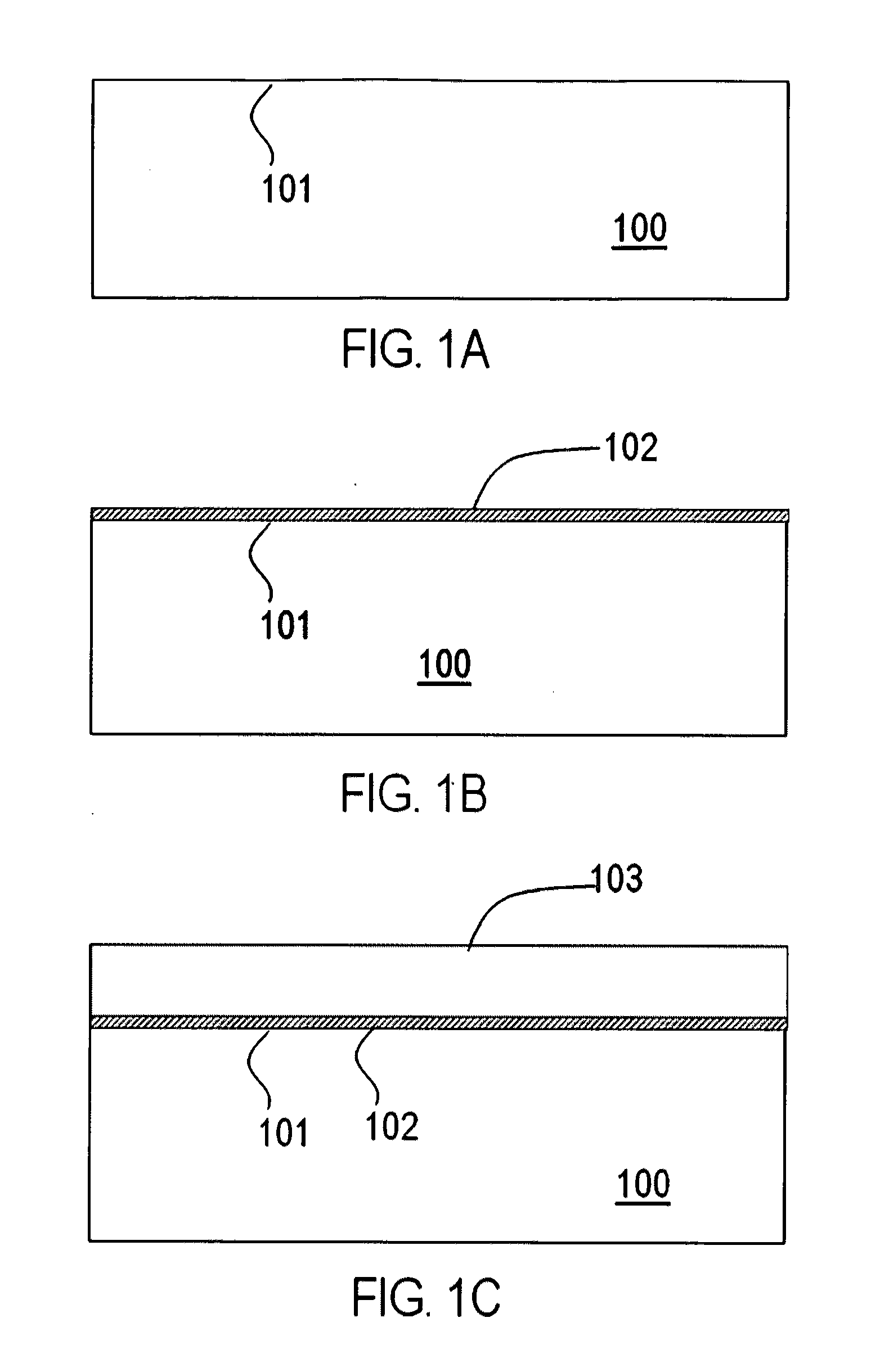
[0032]The following definitions provide additional context for the detailed descriptions that follow and are not intended to limit the scope of the detailed descriptions.

[0033]The term “substrate” as used herein is intended to encompass electronic materials, such as semiconductor and thermoelectric materials, as well as inert materials, such as glasses, ceramics and dielectrics.

[0034]The term “surface” as used herein is intended to encompass an entire surface of a substrate or a selected region of the substrate. For example, the seed layers described herein may be selectively deposited onto regions of the substrate to form discontinuous surfaces for selective metallization.

[0035]The term “metal” as used herein is intended to encompass elemental metals and metal alloys, as well as metallic compounds and metal precursors that can be used to form a conductive contacts and / or nanoparticles.

[0036]The term “self-assembling polymer” as used herein is intended to encompass any polymer that ...


PUM

PropertyMeasurementUnit
Fractionaaaaaaaaaa
Fractionaaaaaaaaaa
Fractionaaaaaaaaaa

Abstract

Methods of forming a conductive metal layers on substrates are disclosed which employ a seed layer to enhance bonding, especially to smooth, low-roughness or hydrophobic substrates. In one aspect of the invention, the seed layer can be formed by applying nanoparticles onto a surface of the substrate; and the metallization is achieved by electroplating an electrically conducting metal onto the seed layer, whereby the nanoparticles serve as nucleation sites for metal deposition. In another approach, the seed layer can be formed by a self-assembling linker material, such as a sulfur-containing silane material.

Description

STATEMENT REGARDING U.S. GOVERNMENT RIGHTS[0001]This invention was made with U.S. government support under Grant No. DE-FG02-08ER46516, awarded by the U.S. Department of Energy (DOE) and Grant No. CMMI-0833084, awarded by the National Science Foundation (NSF). The U.S. Government has certain rights in the invention.BACKGROUND OF THE INVENTION[0002]Metallization is the process of depositing metal material on the surface of a substrate. Electroplating and other forms of electro-deposition are commonly used metallization techniques to form electrical conductive contacts or protective coatings. For example, electroplating is used in ultra large-scale integration (ULSI) to provide multiple levels of copper or copper alloy metallization.[0003]Metallization is also used in the fabrication of optoelectronic devices such as transparent thin film transistors (TFT), flat panel displays, light-emitting diodes (LED), photovoltaic cells, and electrochromic windows to provide interconnects for tra...

Claims


Application Information

Patent Timeline
IPC IPC(8): C25D5/10C25D5/02C25D5/54
CPCC25D5/022C25D5/54C25D5/10
Inventor FENG, HSIEN-PINGCHEN, GANGBO, YUREN, ZHIFENGCHEN, SHUOPOUDEL, BED
Owner GMZ ENERGY
Why Eureka
Try Eureka