Forming method of grid oxidation layer

A technology of gate oxide layer and gate oxide, which is applied in the direction of electrical components, semiconductor/solid-state device manufacturing, semiconductor devices, etc., can solve the problem of reducing the probability of carrier capture, etc., to suppress thermionic effect and reduce interface defects , reducing the effect of silicon dangling bonds

Inactive Publication Date: 2012-06-06
SEMICONDUCTOR MANUFACTURING INTERNATIONAL (BEIJING) CORP
View PDF5 Cites 27 Cited by
  • Summary
  • Abstract
  • Description
  • Claims
  • Application Information

AI Technical Summary

Problems solved by technology

However, these improvements do not involve reducing the probability of carrier capture in the oxide layer, that is, how to effectively impro

Method used


Image

  • Forming method of grid oxidation layer
  • Forming method of grid oxidation layer
  • Forming method of grid oxidation layer

Examples


Embodiment Construction

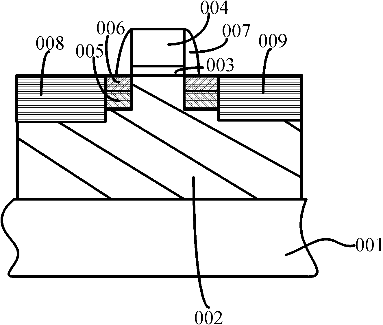
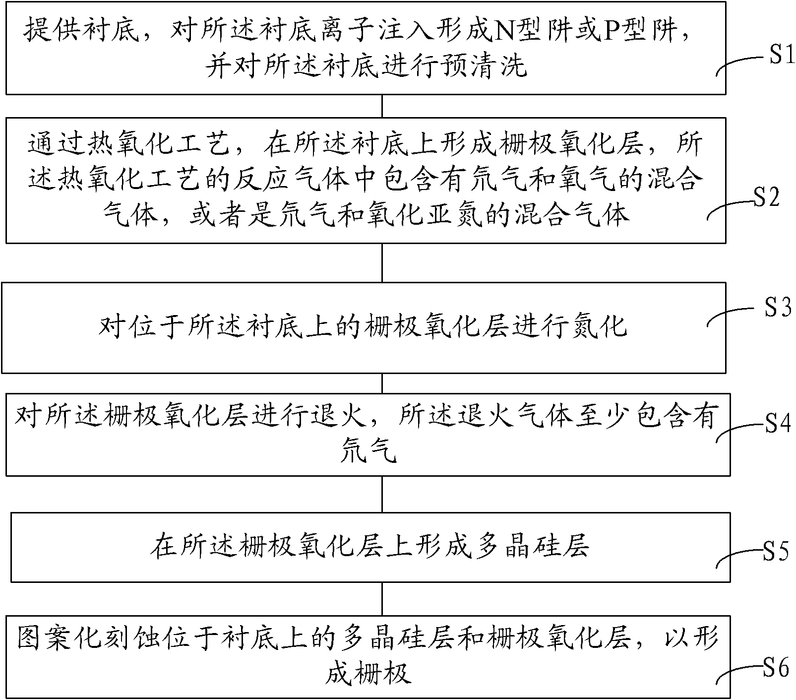
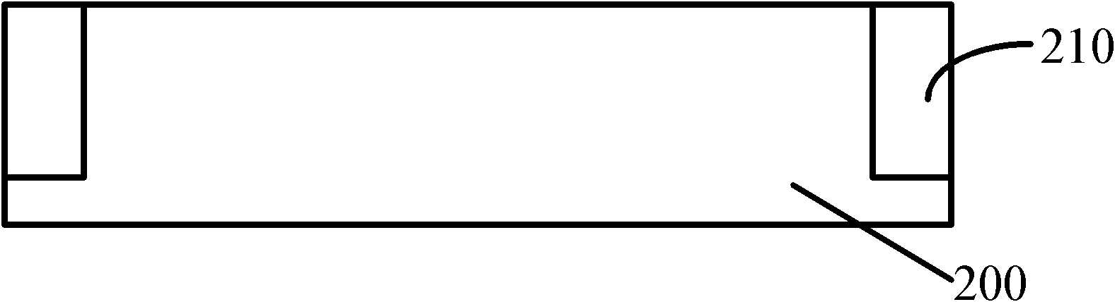
[0024] As the device size shrinks, the thickness of the gate oxide layer becomes correspondingly thinner at the same time. However, when the thickness is reduced to a certain extent, the gate oxide layer is too thin to provide sufficient electrical isolation between the gate conductive material and the underlying semiconductor substrate. More importantly, a thinner gate oxide tends to allow implanted dopant ions to diffuse into the gate oxide. Further, through the semiconductor process environment, the interface between the gate oxide layer and the silicon substrate contains a large number of silicon dangling bonds, and interface defects are formed in the gate oxide layer, making the silicon dangling bonds easy to capture electrons, resulting in hot electrons effect; the silicon dangling bond may also bond with hydrogen in the thermal oxidation process, the silicon-hydrogen bond is weak, and it is easy to break the bond in an external stress environment, and the silicon dangli...


PUM


Abstract

The invention provides a forming method of a grid oxidation layer. The forming method comprises the following steps of: providing a substrate, and forming a grid oxide layer on the substrate by a thermal oxidation process, wherein reactive gas in the thermal oxidation process is mixed gas at least containing deuterium. According to the forming method, a deuterium element is introduced into the thermal-oxidation growth process of the grid oxidation layer, silicon dangling bonds in a saturated interface state form silicon-deuterium bonds with stronger combination so as to reduce the silicon dangling bonds positioned in the interface state or replace hydrogen of silicon-hydrogen bonds to further form the silicon-deuterium bonds with stronger combination. Simultaneously, the silicon-deuterium bond energy is more than the silicon-hydrogen bond energy; and under the semiconductor process environment, the silicon-deuterium bonds are not easily broken due to external stress, so that the silicon dangling bonds positioned in the interface state are further reduced, the interface defects are reduced, and further the hot-electron effect is restrained.

Description

technical field [0001] The invention relates to the field of semiconductor manufacturing, in particular to a method for forming a gate oxide layer. Background technique [0002] The main device in an integrated circuit, especially a VLSI, is a Metal Oxide Semiconductor (MOS for short). Since the invention of the integrated circuit, its performance and function have advanced by leaps and bounds, and the geometric size of the MOS device has been continuously reduced, and its feature size has entered the nanometer scale. [0003] In the process of scaling down the MOS device, the drain voltage does not decrease accordingly, which leads to the increase of the electric field in the channel region between the source and the drain. These electrons are called hot electrons, which will be injected into the gate dielectric layer, thereby causing hot electron effect. This effect belongs to the small size effect of the device, which will cause gate electrode current and semiconductor ...

Claims


Application Information

Patent Timeline
IPC IPC(8): H01L21/28H01L21/316H01L21/336
Inventor 何永根
Owner SEMICONDUCTOR MANUFACTURING INTERNATIONAL (BEIJING) CORP
Why Eureka
Try Eureka