Selective arrangement method of discrete nano-material

A nanomaterial, selective technology that can be used in metal coating processes, processes for creating decorative surface effects, decorative arts, etc., to solve problems such as lack, low cost, and limitations of nanomaterials or substrates

Active Publication Date: 2012-06-13
NANJING UNIV
View PDF6 Cites 4 Cited by
  • Summary
  • Abstract
  • Description
  • Claims
  • Application Information

AI Technical Summary

Problems solved by technology

[0003] Previously, scientists have explored many methods of aligning and integrating nanomaterials, such as electric field induction, fluid flow guidance, LB film method, gas-assisted method, imprint transfer method, etc. Materials or substrates have certain limitations, and there is still a lack of a low-cost, large-scale universal alignment method

Method used


Image

  • Selective arrangement method of discrete nano-material
  • Selective arrangement method of discrete nano-material
  • Selective arrangement method of discrete nano-material

Examples


Embodiment Construction

[0023] The specific process of arranging discrete semiconductor nanowires will be described in detail below with reference to the accompanying drawings, and an exemplary embodiment of the present invention will be presented.

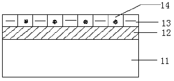
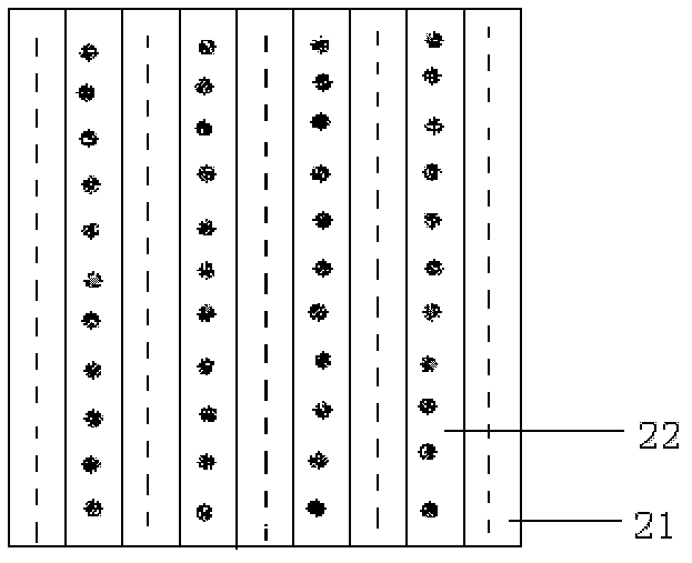
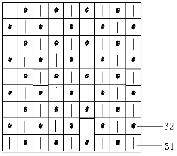
[0024] The structure of the present invention is as attached figure 1 As shown, it includes four parts: a substrate 11 , an oxide layer 12 , a non-polar region 13 and a polar region 14 . In the present invention, the surface of the substrate can be modified into stripe or dot matrix regions by using one-dimensional or two-dimensional phase gratings, as shown in the attached figure 2 , 3 shown. 21 and 22 represent the non-polar and polar regions of the stripe type substrate respectively, and 31 and 32 represent the non-polar and polar regions of the dot matrix type substrate respectively. Striped substrates can be used to arrange linear nanomaterials such as nanowires and nanobelts, and lattice substrates can be used to arrange spherical nanomaterials...


PUM


Abstract

A selective arrangement method of a discrete nano-material comprises steps of: 1) oxidizing a clean substrate, typically a silicon substrate, to obtain a layer of oxide of silicon on a surface of the substrate; 2) placing the oxidized silicon chip into a C6-C8 hydrocarbon solution of octadecyl trichlorosilane and growing a layer of nonpolar OTS self-assembly monomolecular film; 3) etching the nonpolar OTS self-assembly monomolecular film selectively on an objective zone of the substrate by utilizing laser through phase raster; 4) placing the etched silicon substrate in a methanol solution of 3-triethoxy silicyl-1-propylanmine to grow a polar APS self-assembly monomolecular film on the zone etched by the laser and form a polar and nonpolar interval area; and 5) immersing the modified substrate into a nano wire or nano-material fluid suspension and lifting, so as to arrange the nano wire or nano-material according to a rule in the objective polar zone and realize selective arrangement of a discrete semiconductor nano wire. The method has application value.

Description

technical field [0001] The invention relates to a new method for selectively arranging nano materials to form ordered and patterned arrays, which can be used to further prepare various nano material devices to obtain stable and excellent performance. Background technique [0002] In the past ten years, scientists have achieved great success in the preparation of nanomaterials, and have successively obtained various nanomaterials with different shapes, structures, and properties. Most of these nanomaterials have excellent and unique properties and have good applications. prospect. Due to the constraints of growth conditions and various factors, most of the nanomaterials prepared at present are discrete nanomaterials, and there are still many problems in applying them to practical devices. How to arrange and integrate discrete nanomaterials is an extremely important research topic for applying nanomaterials to device fabrication. [0003] Previously, scientists have explored...

Claims


Application Information

Patent Timeline
Patent Type & Authority Applications(China)
IPC IPC(8): B81C1/00
Inventor 施毅高凡盛赟孙华斌潘力佳王剑宇王军转濮林王欣然张荣郑有炓
Owner NANJING UNIV
Why Eureka
Try Eureka