Selective area hetero-epitaxial substrate structure, preparation thereof and epitaxial layer growing method

A technology of heterogeneous epitaxy and substrate structure, applied in the direction of chemical instruments and methods, single crystal growth, single crystal growth, etc., can solve the problems of high cost, complexity, and many processes, so as to simplify the growth steps and process, improve the effective The effect of width

Active Publication Date: 2012-06-13
北京飓芯科技有限公司
View PDF5 Cites 6 Cited by
  • Summary
  • Abstract
  • Description
  • Claims
  • Application Information

AI Technical Summary

Problems solved by technology

Two-step suspended epitaxy technology, the quality of GaN growth in the trench is improved compared with LEO technology, but the central area of ​​each trench is a defect area formed by the connection of adjacent growth fronts
However, the secondary or multiple selected area epitaxial growth based on this has many and complicated processes and high cost, which is not conducive to large-scale production.

Method used


Image

  • Selective area hetero-epitaxial substrate structure, preparation thereof and epitaxial layer growing method
  • Selective area hetero-epitaxial substrate structure, preparation thereof and epitaxial layer growing method
  • Selective area hetero-epitaxial substrate structure, preparation thereof and epitaxial layer growing method

Examples


Embodiment 1

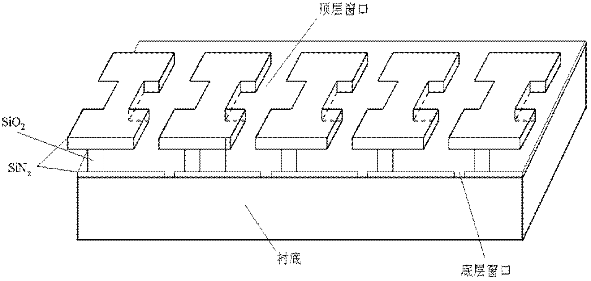
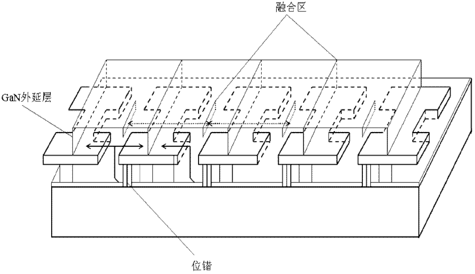
[0036] refer to figure 2 , using the substrate structure to grow GaN epitaxial films. The process is: using metal organic vapor deposition equipment (MOCVD), in hydrogen (H 2 ) atmosphere, with trimethylgallium (trimethylgallium: TMGa) and ammonia (NH 3 ) as the source, grow a 20nm GaN buffer layer on the graphics substrate. Since GaN will not be in SiN x Nucleation occurs on the mask, so the nucleation area will be selected in the underlying window, ie the substrate surface. Next, the growth temperature is raised to 1040° C. to grow a GaN epitaxial layer. The growth process adopts the method of V / III ratio modulation, undergoes "low-high-low-high" pulsed V / III ratio conversion, and grows a GaN epitaxial layer of about 8 μm to ensure the formation of a continuous and flat film.

[0037] The growth process of GaN on the entire substrate structure is as follows: firstly, a 20nm buffer layer is formed in the bottom window, and then the growth in the vertical direction is ca...


PUM

PropertyMeasurementUnit
widthaaaaaaaaaa

Abstract

The invention discloses a selective area hetero-epitaxial substrate structure, a preparation thereof and an epitaxial layer growing method, which belong to the field of photoelectronic technique. The substrate structure comprises a substrate, wherein a bottom mask layer and a top mask layer are sequentially arranged on the substrate, the ground floor mask layer is provided with bar-type windows which are distributed in a periodical mode, the top floor mask layer is provided with cross type windows which are distributed in a periodical mode, and an I-shaped top floor mask area is arranged between the cross type windows. Two ends of the I-shaped top floor mask area at the top are connected with a bar-type mask area of the ground floor mask layer through a fragmented dielectric layer, and the cross type windows at the top and the bar-type windows on the ground floor are staggered. The invention further provides the preparation method of the substrate structure and the epitaxial layer growing method based on the substrate structure. Compared with the prior art, the selective area hetero-epitaxial substrate structure provides a one-step method hetero-epitaxial substrate structure, simplifies growing processes, improves effective width of a dislocation-free epitaxial film simultaneously, and has using value.

Description

technical field [0001] The invention relates to a novel heterogeneous epitaxial growth substrate method, which can be directly applied to grow materials such as high-quality Group III nitride semiconductors. Background technique [0002] Materials are the cornerstone of scientific and technological development. Usually, heteroepitaxial growth has become the basic method widely used in material growth due to the scarcity and difficulty in obtaining matching substrates. Currently, the rapidly developing group III nitride semiconductor materials are mainly epitaxially grown on substrates such as sapphire. The so-called Group III nitride materials, including GaN, AlN, InN and their ternary and quaternary alloys, are all direct bandgap materials, with a wide bandgap range (0.75eV~6.2eV), high breakdown electric field, thermal High conductivity, high electron saturation rate, and chemical corrosion resistance, these excellent optical and electrical properties and excellent mater...

Claims


Application Information

Patent Timeline
Patent Type & Authority Applications(China)
IPC IPC(8): C30B25/18C30B25/04C30B29/38H01L21/02
Inventor 李磊胡晓东刘培基谢亚宏李丁贺永发杨志坚张国义
Owner 北京飓芯科技有限公司
Why Eureka
Try Eureka