Production method of deep groove isolation structure

A technology of isolation structure and manufacturing method, which is applied in semiconductor/solid-state device manufacturing, electrical components, circuits, etc., can solve problems such as poor uniformity in the plane and residual liquid medicine, so as to reduce the difficulty of back-end process and reduce the stability of devices Hidden dangers, the effect of improving in-plane uniformity

Inactive Publication Date: 2012-06-27
SHANGHAI HUAHONG GRACE SEMICON MFG CORP
View PDF5 Cites 4 Cited by
  • Summary
  • Abstract
  • Description
  • Claims
  • Application Information

AI Technical Summary

Problems solved by technology

[0003] Traditional LDMOS devices generally use ordinary STI (deep trench isolation) and thick oxygen isolation. This isolation technology will cause problems such as poor in-plane uniformity and easy to cause liquid residue, which limits the application of RF LDMOS devices to a certain extent. Application on high-speed and high-frequency devices

Method used


Image

  • Production method of deep groove isolation structure
  • Production method of deep groove isolation structure
  • Production method of deep groove isolation structure

Examples


Embodiment Construction

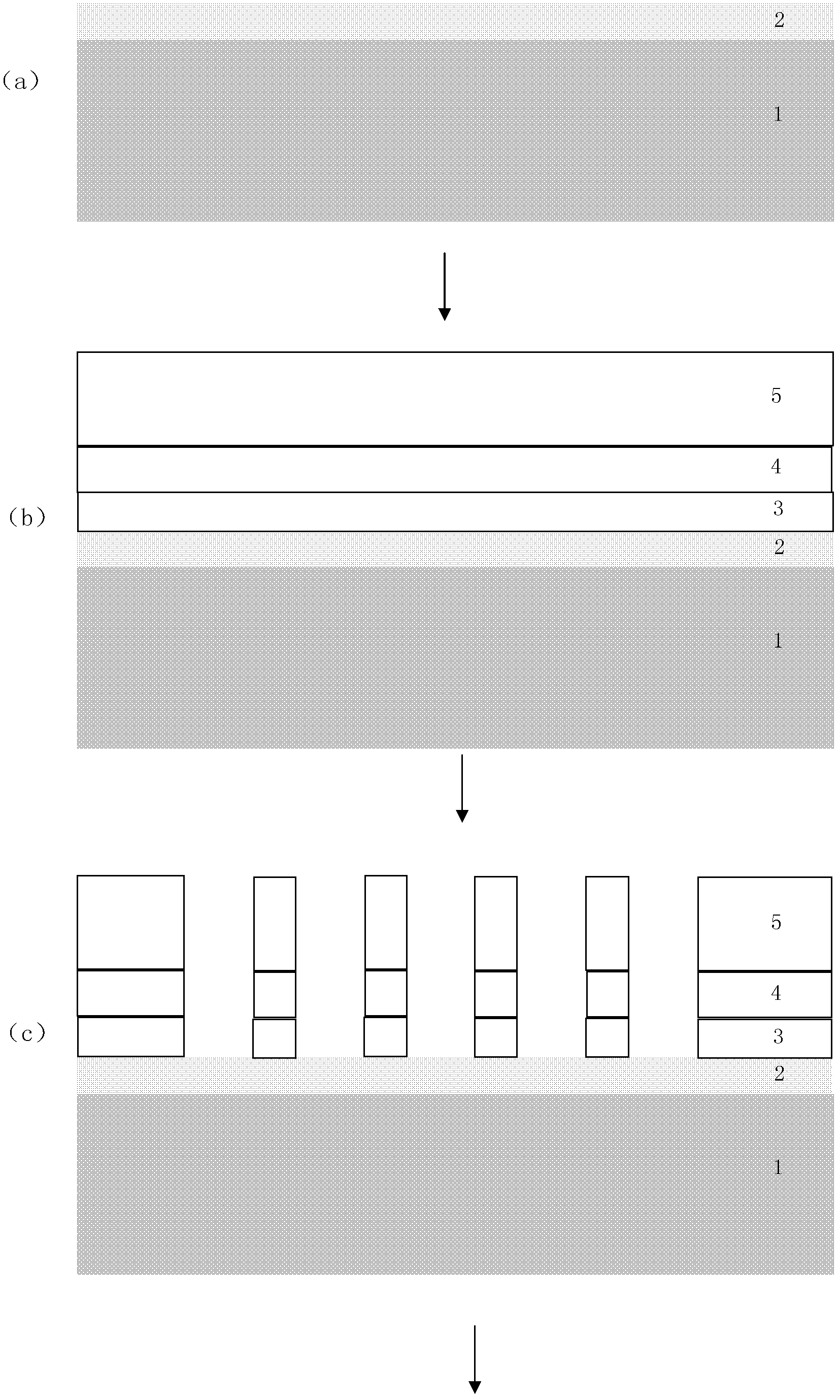
[0021] In order to have a more specific understanding of the technical content, characteristics and effects of the present invention, the manufacturing process flow of the deep trench isolation structure in the RFLDMOS device is described in detail as follows in conjunction with the illustrated embodiment:

[0022] Step 1, growing an epitaxial layer 2 on a silicon substrate 1, such as figure 1 (a) shown.

[0023] Step 2, enter the furnace tube to oxidize, and grow an oxide layer 3 with a thickness of 150-300 angstroms; then enter the furnace tube to grow a layer of silicon nitride 4 with a thickness of 500-800 angstroms; accumulate to form a layer of oxide layer 5 with a thickness of 2000-5000 angstroms, such as figure 1 (b) shown.

[0024] Step 3, exposure, development, using dry etching method, open the area to be etched deep groove, such as figure 1 (c) shown.

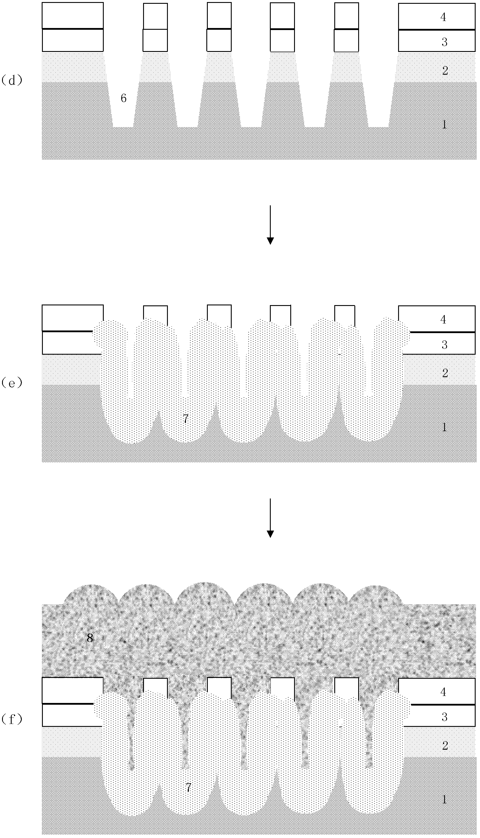
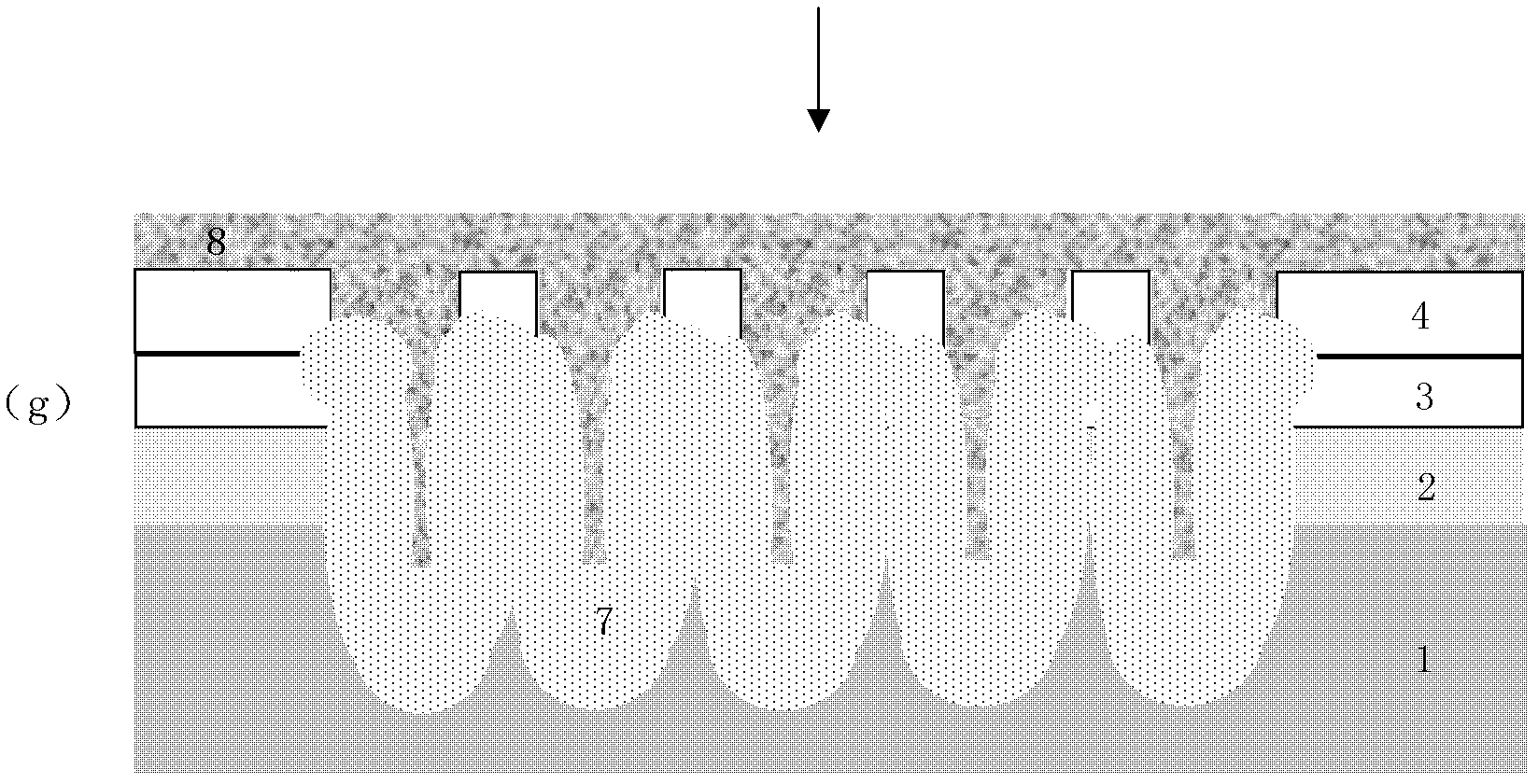
[0025] Step 4, using the oxide layer 3, the silicon nitride 4 and the oxide layer 5 as an etching barrier lay...


PUM


Abstract

The invention discloses a production method of a deep groove isolation structure. After an epitaxial layer is grown, the method produces the deep groove isolation structure in the following steps: 1) growing silicon dioxide and silicon nitride in a furnace tube, and depositing silicon dioxide on silicon nitride; 2) performing exposure and development, and opening an area where a deep groove is to be etched in a dry etching mode; 3) utilizing silicon dioxide-silicon nitride-silicon dioxide formed by the step 1) to serve as an etching blocking layer, and forming the deep groove in the dry etching mode; 4) performing furnace pipe oxidation again, growing silicon dioxide, and fully oxidizing silicon below silicon nitride of a deep groove isolation area; 5) depositing silicon dioxide and sealing an opening of the deep groove; and 6) carrying out planarization of the surface of the deep groove. The method forms an ultra-thick field oxidation isolation layer by means of a deep groove etching and oxidation technology, and utilizes silicon nitride to serve as the blocking layer of planarization, thereby not only achieving isolation effect, but also greatly improving evenness in the surface and reducing difficulty of rear-end process.

Description

technical field [0001] The invention relates to the field of manufacturing semiconductor integrated circuits, in particular to a method for manufacturing a deep trench isolation structure. Background technique [0002] RF LDMOS power devices due to good electrical characteristics (for example, high linearity, high gain, high output power, high thermal stability, high operating voltage, simple bias circuit, constant input impedance, etc.) and compatibility with existing CMOS integrated circuit technology Good compatibility, has been widely used in the field of wireless communication. [0003] Traditional LDMOS devices generally use ordinary STI (deep trench isolation) and thick oxygen isolation. This isolation technology will cause problems such as poor in-plane uniformity and easy to cause liquid residue, which limits the application of RF LDMOS devices to a certain extent. Applications on high-speed high-frequency devices. Contents of the invention [0004] The technica...

Claims


Application Information

Patent Timeline
Patent Type & Authority Applications(China)
IPC IPC(8): H01L21/762
Inventor 遇寒梅绍宁
Owner SHANGHAI HUAHONG GRACE SEMICON MFG CORP
Why Eureka
Try Eureka