e/LQFP (low-profile quad flat package) planar packaging part with grounded ring and production method of e/LQFP planar packaging part with grounded ring

A production method and a grounding ring technology, which are applied in semiconductor/solid-state device manufacturing, semiconductor/solid-state device components, electrical components, etc., can solve the problem of large chip bonding, non-stick carrier silver plating area, easy-to-scan separation layer, etc. problem, to achieve the effect of increasing bonding force, high reliability and test yield, and improving reliability and test yield

Active Publication Date: 2012-06-27
TIANSHUI HUATIAN TECH +1
View PDF6 Cites 11 Cited by
  • Summary
  • Abstract
  • Description
  • Claims
  • Application Information

AI Technical Summary

Problems solved by technology

[0005] In order to overcome the problems existing in the above-mentioned prior art, the object of the present invention is to provide an eLQFP planar package with a grounding ring, which solves the problems of the existing eLQFP package that the chip is larger and the wire is not sticky and the chip is smaller. The silver zone is prone to the problem of scanning detachment

Method used


Image

  • e/LQFP (low-profile quad flat package) planar packaging part with grounded ring and production method of e/LQFP planar packaging part with grounded ring
  • e/LQFP (low-profile quad flat package) planar packaging part with grounded ring and production method of e/LQFP planar packaging part with grounded ring
  • e/LQFP (low-profile quad flat package) planar packaging part with grounded ring and production method of e/LQFP planar packaging part with grounded ring

Examples


Embodiment 1

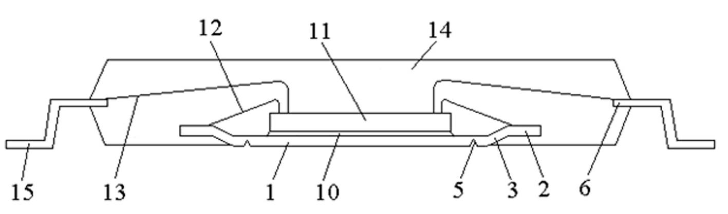
[0088] The wafer is thinned by the existing process method to obtain a thinned wafer with a final thinned thickness of 150 μm; during the thinning process, the rough grinding speed is 5 μm / s, and the thickness of the wafer after rough grinding is 200 μm + film thickness; The fine grinding speed is 0.5μm / s, and the thickness of the wafer after fine grinding is 150μm+the thickness of the film, and the process of preventing chip warpage is adopted when thinning; the DISC 3350 dicing machine is used for scribing; when scribing, the scribing feed is controlled. Speed ​​≤ 10mm / s, and adopts anti-fragmentation, anti-crack scribing process software control technology; use conductive adhesive to paste IC chips, fix IC chips on the die bonding machine, send the lead frame with grounding ring to the feeding table, and paste the chips The machine grabs a lead frame and sends it into the track, and after sending it to the chip bonding table, apply conductive glue on the carrier 1. The condu...

Embodiment 2

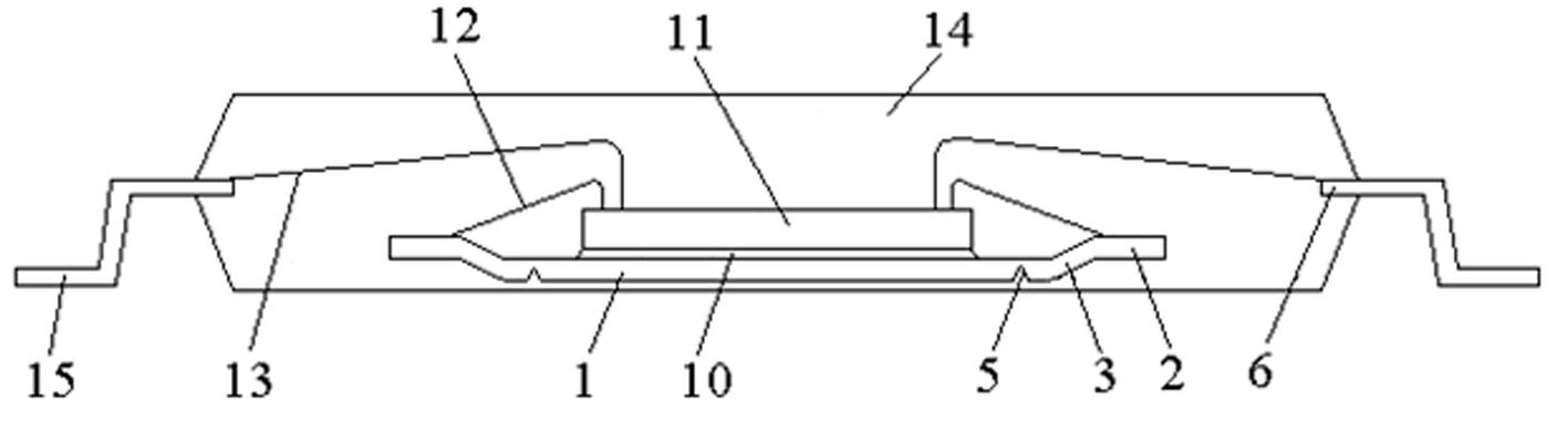
[0090] The wafer is thinned by the existing process method to obtain a thinned wafer with a final thinning thickness of 200 μm; during the thinning process, the rough grinding speed is 3 μm / s, and the thickness of the wafer after rough grinding is 250 μm + film thickness The fine grinding speed is 0.8μm / s, and the thickness of the wafer after fine grinding is 200μm+the thickness of the film, and the process of preventing chip warpage is adopted when reducing the thickness; the double-knife dicing machine is used for scribing; Knife speed ≤ 10mm / s, and adopts anti-fragmentation, anti-crack scribing process software control technology; use insulating glue to paste IC chips, fix IC chips on the chip bonding machine, send the lead frame with grounding ring to the feeding table, stick The chip machine grabs a lead frame and sends it into the track, and after sending it to the bonding table, apply insulating glue on the carrier 1. The insulating glue is the first bonding material 10,...

Embodiment 3

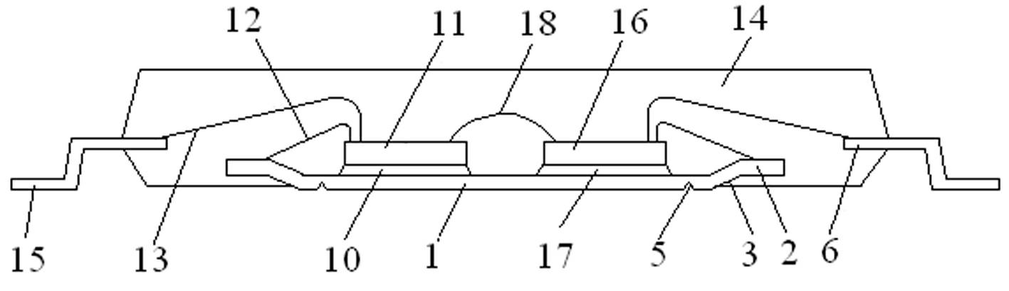
[0092] The wafer is thinned by the existing process method to obtain a thinned wafer with a final thinning thickness of 175 μm; during the thinning process, the rough grinding speed is 4 μm / s, and the thickness of the wafer after rough grinding is 225 μm + film thickness ;Finish grinding speed is 0.5μm / s, the thickness of the wafer after fine grinding is 175μm+film thickness, the process of preventing chip warping is adopted when thinning; A-WD-300TXB dicing machine is used for scribing; when scribing, control Scribing feed speed ≤10mm / s, and adopts anti-fragmentation and anti-crack scribing process software control technology; uses adhesive film to paste IC chip, and puts the IC chip with adhesive film directly through the adhesive film chip loading machine On the carrier 1, the IC chip is bonded to the carrier 1, and the IC chip is the first IC chip 11, and a lead frame is glued and delivered to the receiving box; after bonding all the first IC chips 11 of this batch in the s...


PUM


Abstract

The invention discloses an e/LQFP (low-profile quad flat package) planar package with a grounded ring, which comprises a carrier and the grounded ring, wherein one to two IC (integrated circuit) chips are adhered to the carrier. The IC chips are connected with an inner pin through bonding wires, the inner pin is connected with an outer pin, the lower end face of the grounded ring is higher than the upper end face of the carrier, and the carrier is connected with the grounded ring through a ribbed plate. The end face, without the IC chips, of the carrier is provided with an anti-overflow ring, the grounded ring, the bonding wires, the ribbed plate and the inner pin are packaged in a plastic packaging part which is fixedly packaged on the carrier, the outer pin is positioned outside the plastic packaging part, the outer pin and the plastic packaging part are coplanar, and the lower end face of the carrier is positioned outside the plastic packaging part or packaged inside the plastic packaging part. The e/LQFP planar package with the grounded ring is produced by procedures of wafer thinning, scribing, coring, bonding and the like. Layering or shedding of a ground wire caused by making the ground wire on the carrier can be avoided, the carrier is free of silver coating, and packaging reliability is improved.

Description

technical field [0001] The invention belongs to the technical field of electronic information component manufacturing, and relates to an e / LQFP planar package with a grounding ring, and also relates to a production method of the planar package. Background technique [0002] Since the 1980s, electronic products have developed in the direction of multi-functionality, thinness and shortness, and the requirements for high-speed and high-density packaging technology have been put forward. Therefore, SMT packaging has been developed. The representative forms of SMT packaging are: PLCC, SOP, SOJ, TSOP, TSSOP, PQFP, QFJ, LQFP, TQFP, etc. [0003] LQFP (LOW-Profile Quad package) is a square flat packaging technology (QFP) with a package height of 1.4mm. It is suitable for thin product packaging with high density and fine pitch. It belongs to the packaging technology of mid-range products. It is often used in CP packaging and is easy to operate. , high reliability, small size, small ...

Claims


Application Information

Patent Timeline
Patent Type & Authority Applications(China)
IPC IPC(8): H01L25/00H01L23/495H01L23/31H01L21/60H01L21/56
CPCH01L2224/48137H01L2224/73265H01L2224/32245H01L2224/48247H01L2924/14H01L2924/181H01L24/73H01L2224/45144H01L2224/45147H01L2224/48091H01L2224/48257H01L2924/00012H01L2924/00014H01L2924/00
Inventor 李习周慕蔚郭小伟李存满
Owner TIANSHUI HUATIAN TECH
Why Eureka
Try Eureka