Production method of multi-stage HDI plate

A production method and core board technology, applied in multilayer circuit manufacturing, electrical components, printed circuits, etc., can solve problems such as blind hole mismatch, inconsistent drilling and buried hole coefficients, etc., achieve good dimensional stability and shorten production The effect of cycle time and production cost saving

Active Publication Date: 2012-06-27
SHENZHEN SUNTAK MULTILAYER PCB
View PDF5 Cites 36 Cited by
  • Summary
  • Abstract
  • Description
  • Claims
  • Application Information

AI Technical Summary

Problems solved by technology

[0005] In view of the above problems, the purpose of the present invention is to provide a production method for multi-level HDI boards, to solve the problem that existing multi-level HDI boards make inner layer blind holes and buried holes using the same group of holes as positioning holes for separate drilling. The coefficient of drilling buried holes is inconsistent with the coefficient of blind holes, and the problem that through holes and blind holes do not match

Method used


Image

  • Production method of multi-stage HDI plate
  • Production method of multi-stage HDI plate
  • Production method of multi-stage HDI plate

Examples


Embodiment Construction

[0033] In order to illustrate the idea and purpose of the present invention, the present invention will be further described below in conjunction with the accompanying drawings and specific embodiments.

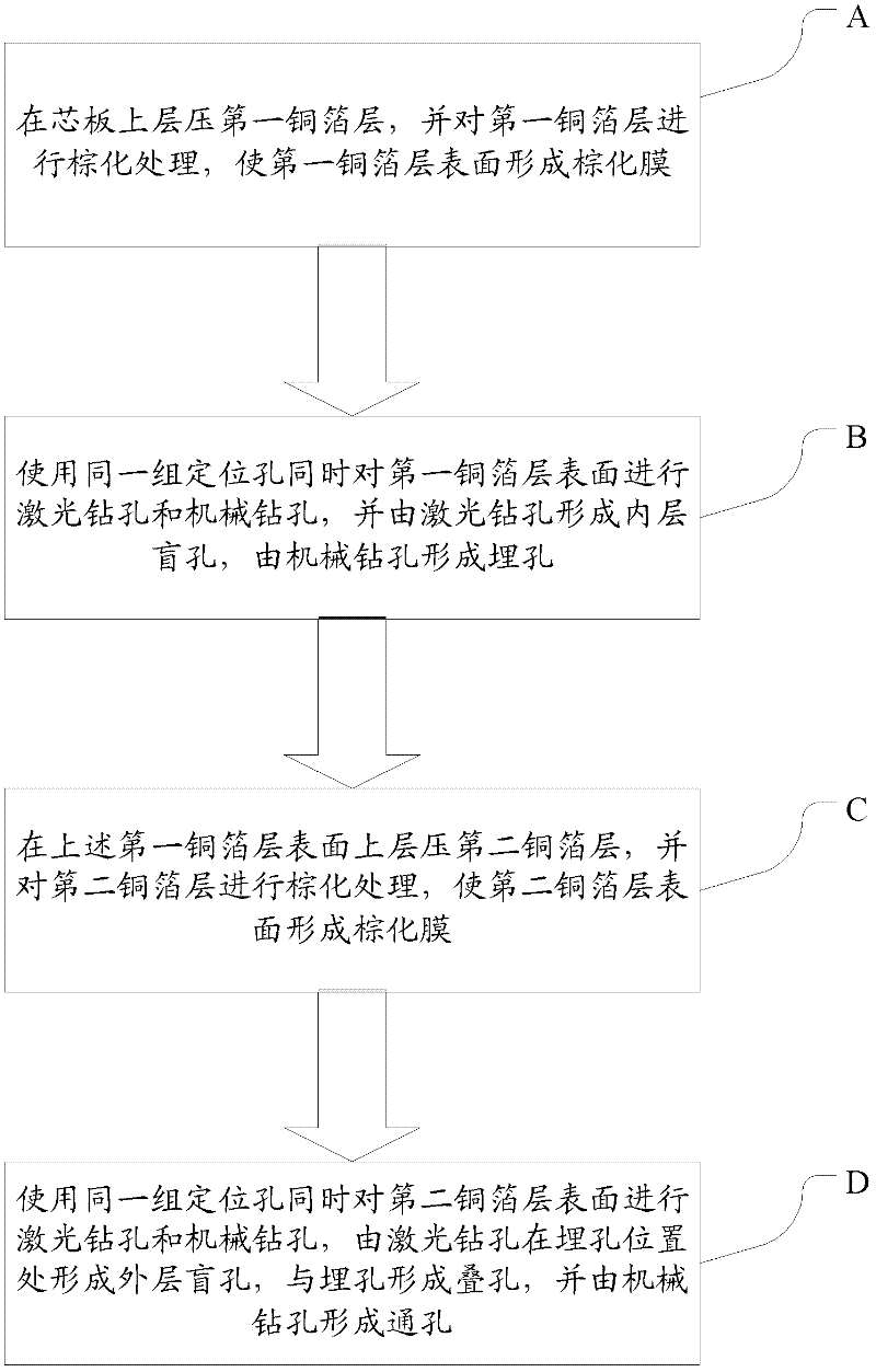
[0034] The present invention provides a method for producing multi-stage HDI boards, which is mainly used to solve the problem of multiple blind holes, buried holes, through holes, or both buried and blind holes in the production process of current multi-stage HDI boards. , it is prone to the problem of mismatching through holes and blind holes.

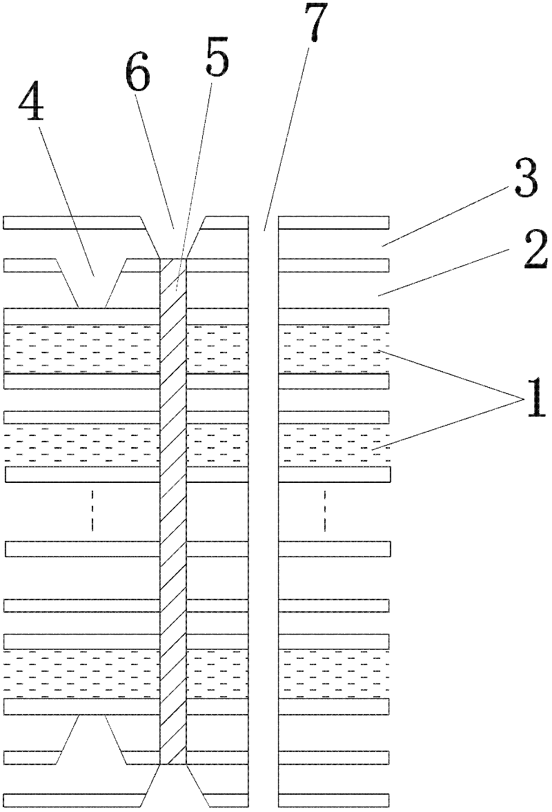
[0035] See figure 1 as shown, figure 1 It is a structural schematic diagram of laser blind holes, buried holes and through holes on a multilayer circuit board of the present invention.

[0036] Inside is the core board 1, the first layer above the core board 1 is the first copper foil layer 2, and above the first copper foil layer 2 is the second copper foil layer 3, wherein on the first copper foil layer 2 The inner layer blind ...


PUM

PropertyMeasurementUnit
pore sizeaaaaaaaaaa

Abstract

The invention discloses a production method of a multi-stage HDI plate. The method comprises the following steps: A. laminating a first copper foil layer on a core plate, carrying out multiband to the first copper foil layer so as to form a brown film on a surface of the first copper foil layer; B. using a same group of location holes to simultaneously carry out laser drilling and mechanical drilling to the surface of the first copper foil layer, forming an internal-layer blind hole through the laser drilling and forming a buried hole through the mechanical drilling; C. laminating a second copper foil layer on the surface of the first copper foil layer, carrying out the multiband to the second copper foil layer so as to form the brown film on the surface of the second copper foil layer; D. using the same group of location holes to simultaneously carry out the laser drilling and the mechanical drilling to the surface of the second copper foil layer, forming an outer-layer blind hole on the position of the buried hole through the laser drilling, forming a folded hole with the buried hole and forming a through hole through the mechanical drilling. At present, the blind hole and the buried hole are drilled separated so that the through hole and the blind hole are not matched with each other. According to the method of the invention, the above problem can be solved; processes of internal layer copper deposition, padpower, an internal layer plating hole graph, porefilling electroplating, film stripping, abrasive-belt grinding plate and the like can be reduced; a production period can be substantially shortened and production cost can be saved.

Description

Technical field: [0001] The invention relates to a production method of a multi-stage HDI board, in particular to a production method of a multi-stage HDI board in which multiple buried holes, blind holes or buried holes and blind holes exist simultaneously. Background technique: [0002] HDI circuit board is also called high-density interconnection board, which means that the aperture is below 6mil, the ring diameter of the ring (Hole Pad) is below 0.25mm, the contact density is above 130 points / square, and the line width / spacing is below 3mil / 3mil printed circuit board. HDI circuit boards can reduce the production cost of multi-layer PCB boards, increase circuit density, and have the advantages of high reliability and good electrical performance. [0003] Due to the continuous increase in the number of laser-drilled HDI boards and the complexity of the structure, the production process of multi-order HDI boards has increased, the scrap rate has increased, and the producti...

Claims


Application Information

Patent Timeline
Patent Type & Authority Applications(China)
IPC IPC(8): H05K3/46
CPCH05K3/429H05K3/46H05K2201/09536H05K2201/09509H05K3/0047H05K3/4652H05K3/0035H05K2201/096
Inventor 姜雪飞黄海蛟杜明星林楠白亚旭
Owner SHENZHEN SUNTAK MULTILAYER PCB
Why Eureka
Try Eureka