SOI (silicon on insulator) based electrooptical modulator based on symmetrical and vertical grating coupling

An electro-optical modulator and vertical coupling technology, which is applied in instruments, optics, nonlinear optics, etc., can solve problems such as large size and insertion loss, process and temperature sensitivity, and large optical bandwidth.

Active Publication Date: 2012-07-04
INST OF SEMICONDUCTORS - CHINESE ACAD OF SCI
View PDF4 Cites 28 Cited by
  • Summary
  • Abstract
  • Description
  • Claims
  • Application Information

AI Technical Summary

Problems solved by technology

Compared with microring modulation devices, MZ modulators have larger size, insertion loss, and higher power consumption, but they are not as sensitive to process and temperature as microring devices, and they also have larger optical bandwidths.

Method used


Image

  • SOI (silicon on insulator) based electrooptical modulator based on symmetrical and vertical grating coupling
  • SOI (silicon on insulator) based electrooptical modulator based on symmetrical and vertical grating coupling
  • SOI (silicon on insulator) based electrooptical modulator based on symmetrical and vertical grating coupling

Examples


Embodiment Construction

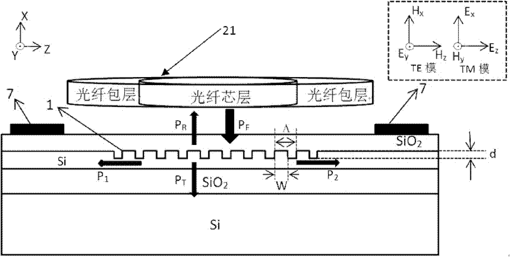
[0021] Since the present invention is a silicon-based electro-optical modulator based on SOI substrate material design, for different buried oxide layer thicknesses and top layer silicon thicknesses, the corresponding optimal design is also different to achieve functional requirements. Therefore, for convenience of description, the substrate of the present invention The bottom material defaults to specific implementation parameters, that is, the thickness of the buried oxide layer is 2 μm, and the thickness of the top silicon layer is 220 nm.

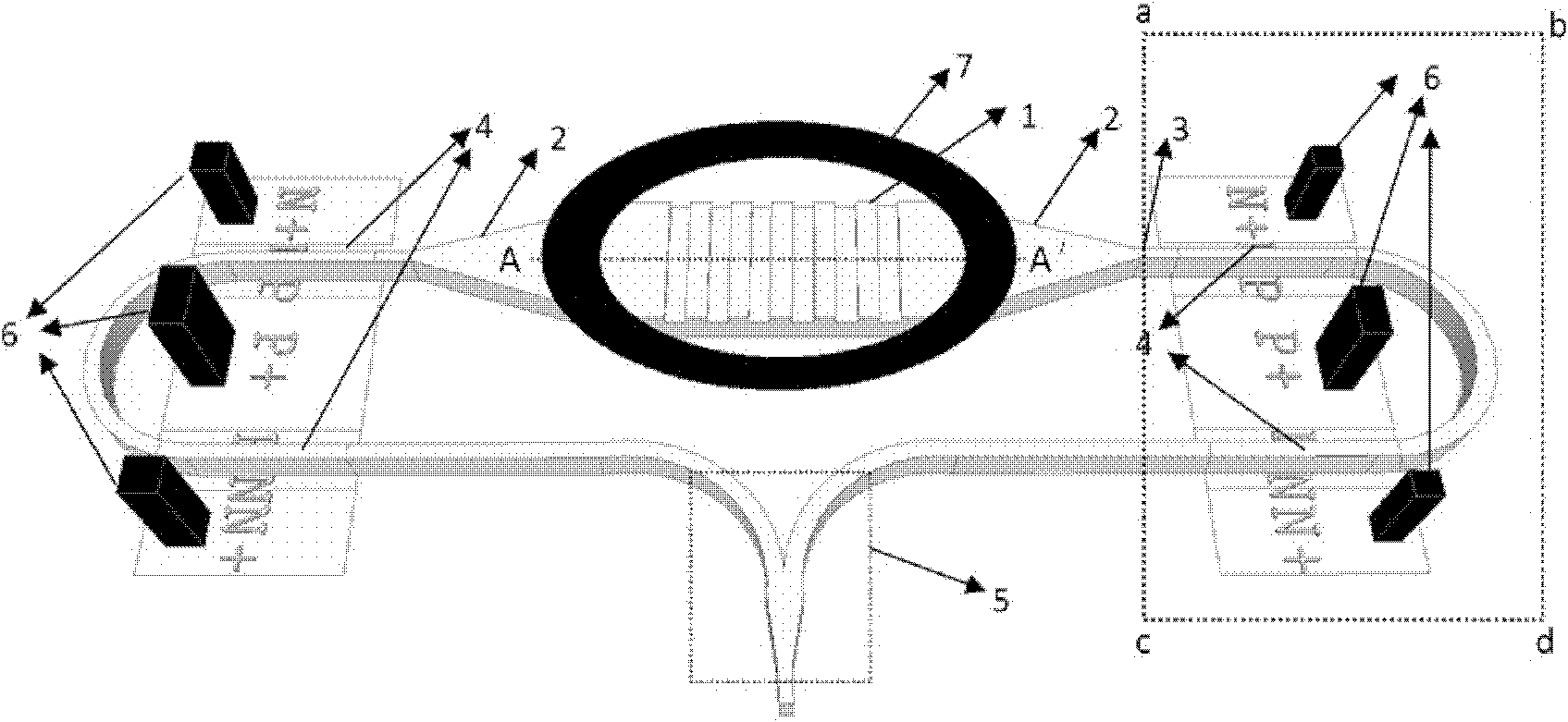
[0022] see figure 1 and figure 2 , the present invention provides an SOI-based electro-optic modulator based on symmetrical vertical grating coupling, comprising:

[0023] A symmetrical vertical coupling grating 1, as SOI-based electro-optic modulator and optical fiber 21 ( figure 2 ) interface or coupler and 3-dB optical beam splitter at the input of the SOI-based electro-optic modulator;

[0024] Two mode converters 2, as the con...


PUM

PropertyMeasurementUnit
diameteraaaaaaaaaa
thicknessaaaaaaaaaa
thicknessaaaaaaaaaa

Abstract

The invention discloses an SOI (silicon on insulator) based electrooptical modulator based on symmetrical and vertical grating coupling, which comprises a symmetrical and vertical coupling grating, a 3-d B optical beam splitter, two mode converters, two optical phase shift arms, an optical beam combiner, two coplanar waveguide wave traveling electrodes and an annular metal alignment mark, wherein the 3-d B optical beam splitter acts as an interface of the SOI based electrooptical modulator and a single mode fiber or an input end of a coupler and the SOI based electrooptical modulator; the two mode converters act as the connection of a wide wave guide of the symmetrical and vertical coupling grating and a single mode ridge-shaped waveguide; each optical phase shift arm consists of the single mode ridge-shaped waveguide and an electric structure embedded into the single mode ridge-shaped waveguide; the optical beam combiner is used for combining the light in the two optical phase shift arms which are divided by the symmetrical and vertical coupling grating into one beam, thus phase modulation of light is converted into intensity modulation; the coplanar waveguide wave traveling electrodes are respectively positioned on the two optical phase shift arms, form electric contact with the electric structure in the optical phase shift arms, and are used for the loading and transmission of radio frequency / micro wave electrical modulation signals; and the annular metal alignment mark is positioned around the symmetrical and vertical coupling grating, and is used for the alignment of the optical fiber in an optical grating test.

Description

technical field [0001] The invention relates to silicon-based photonics and chip-level optical interconnection technology, in particular to an SOI-based electro-optic modulator based on symmetrical vertical grating coupling. Background technique [0002] Microelectronics technology and optical fiber communication technology are the two cornerstones of human information society. In the past half century, with the development of integrated circuits, silicon-based materials and device technology have become surprisingly mature, and with the continuous shrinking of process feature sizes, the integration of integrated circuits has been developing rapidly in accordance with Moore's law. The higher integration of chips brings not only an increase in the number of transistors, but also an increase in chip functions and processing speed. For example, the latest 8-core microprocessor Nehalem-EX of Intel's 45nm process has 2.3 billion transistors. However, as feature sizes shrink and...

Claims


Application Information

Patent Timeline
Patent Type & Authority Applications(China)
IPC IPC(8): G02F1/025
Inventor 陈弘达张赞允黄北举张赞
Owner INST OF SEMICONDUCTORS - CHINESE ACAD OF SCI
Why Eureka
Try Eureka