Large-scale indium column generation method for infrared focal plane detector

An infrared focal plane and growth method technology, which is applied in the field of indium column growth of large-scale infrared focal plane detectors, can solve the problems of blind elements in the detector and easy residues in the indium column, and achieve good shape consistency and improve connectivity Rate, reduce the effect of blind rate

Inactive Publication Date: 2012-07-04
11TH RES INST OF CHINA ELECTRONICS TECH GROUP CORP
View PDF4 Cites 10 Cited by
  • Summary
  • Abstract
  • Description
  • Claims
  • Application Information

AI Technical Summary

Problems solved by technology

[0005] The present invention provides a large-scale infrared focal plane detector indium column growth method, which is used to solve the problem that the b

Method used


Image

  • Large-scale indium column generation method for infrared focal plane detector
  • Large-scale indium column generation method for infrared focal plane detector
  • Large-scale indium column generation method for infrared focal plane detector

Examples


Embodiment 1

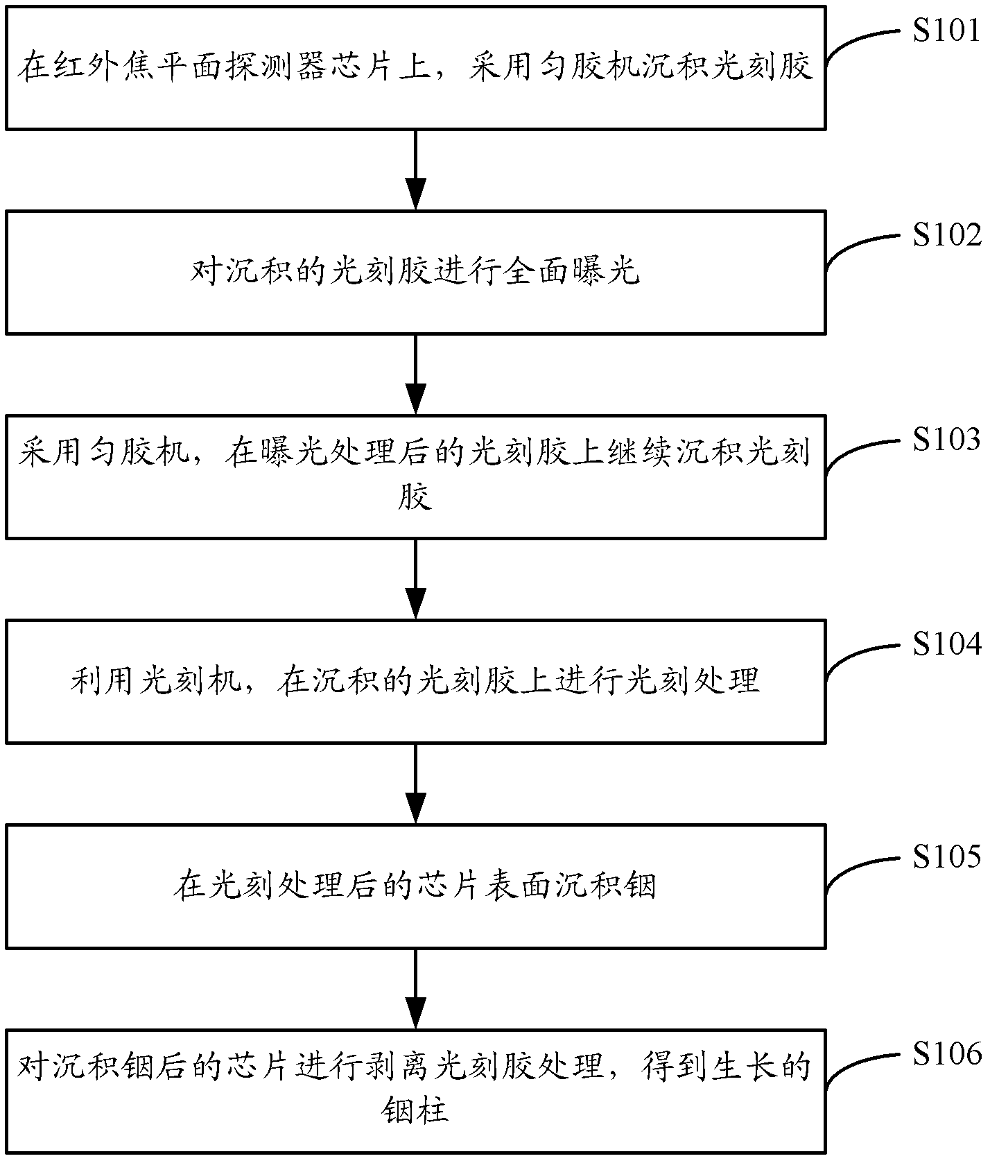
[0033] An embodiment of the present invention provides a large-scale infrared focal plane detector indium column growth method, such as figure 1 shown, including the following steps:

[0034] Step S101, depositing photoresist on the infrared focal plane detector chip by using a coater;

[0035] In this step, the photoresist is deposited with a thickness of 10-20 microns.

[0036] Step S102, fully exposing the deposited photoresist;

[0037] In this step, the exposure time for full exposure is 15-30s;

[0038] In this step, the method of fully exposing the deposited photoresist is preferably but not limited to: placing the chip on which the photoresist is deposited on a photolithography machine, and using the photolithography machine to expose the coated photoresist without installing a photoresist plate. The photoresist is exposed to light.

[0039] Step S103, using a coater to continue depositing photoresist on the exposed photoresist;

[0040] In this step, the photores...

Embodiment 2

[0048] An embodiment of the present invention provides a method for growing an indium column for a large-scale infrared focal plane detector, which is a specific implementation of the method described in Embodiment 1. The method described in this embodiment includes:

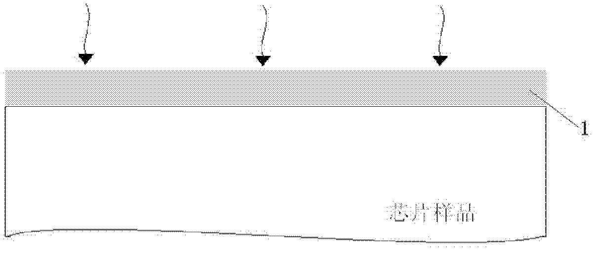
[0049] Step 1, on the infrared focal plane detector chip, use a homogenizer to deposit a photoresist with a thickness of 12 μm; the chip for depositing the photoresist is as follows figure 2 As shown, "1" in the figure is the photoresist.

[0050] In step 2, the chip deposited with photoresist is placed on the exposure table of the exposure machine, and the photoresist is exposed by using the photolithography machine without a photoresist plate; in this embodiment, the exposure time is 20s.

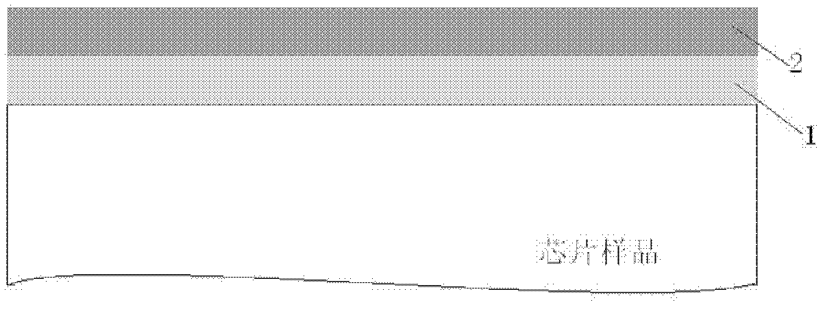
[0051] Step 3: Deposit a photoresist with a thickness of 12 μm on the chip by using a homogenizer; the chip where the photoresist is deposited again is as follows image 3 As shown, "2" in the figure represents the photor...


PUM

PropertyMeasurementUnit
Thicknessaaaaaaaaaa

Abstract

The invention discloses a large-scale indium column generation method for an infrared focal plane detector. The large-scale indium column generation method comprises the following steps of: step 1, coating photoresist for a set thickness on a chip of the infrared focal plane detector; step 2, carrying out blanket exposure treatment on the coated photoresist; step 3, continuously coating the photoresist for the set thickness on the exposed photoresist; step 4, photoetching the coated photoresist by using a photoetching machine; and step 5, depositing indium on the chip of the infrared focal plane detector after photoetching and then stripping the photoresist, so as to obtain the generated indium column. According to the method provided by the invention, the indium column is stripped by using two layers of the photoresist, so that the indium column has no residues at the bottom and has good appearance consistency. Furthermore, the communication rate of reverse welding of the chip of the detector and a read-out circuit can be effectively improved, and the blind pixel rate of the detector is effectively reduced.

Description

technical field [0001] The invention relates to the technical field of semiconductors, in particular to a method for growing an indium column of a large-scale infrared focal plane detector. Background technique [0002] At present, infrared focal plane detection technology has been widely used in various fields due to its remarkable advantages such as wide spectral response band, more target information, and day and night work. [0003] At present, the domestic mainstream focal plane detectors use the readout circuit to read out the signal, and the detector array chip and the readout circuit are integrated with the interconnection of indium pillars. Nowadays, with the rapid development of focal plane detectors, it is necessary to prepare detector chips with larger arrays and better imaging effects. The size of the device chip will not increase exponentially, which means that the bottom area of ​​the indium column will also decrease with the reduction of the pixel pitch. ...

Claims


Application Information

Patent Timeline
IPC IPC(8): H01L31/18
CPCY02P70/50
Inventor 白谢辉郭喜支淑英
Owner 11TH RES INST OF CHINA ELECTRONICS TECH GROUP CORP
Why Eureka
Try Eureka