Light emitting diode crystal grains and manufacturing method thereof
A technology of light-emitting diodes and manufacturing methods, which is applied in semiconductor/solid-state device manufacturing, electrical components, circuits, etc., and can solve problems such as reducing the light-emitting efficiency of light-emitting diode grains
- Summary
- Abstract
- Description
- Claims
- Application Information
AI Technical Summary
Problems solved by technology
Method used
Image

Examples
no. 1 example
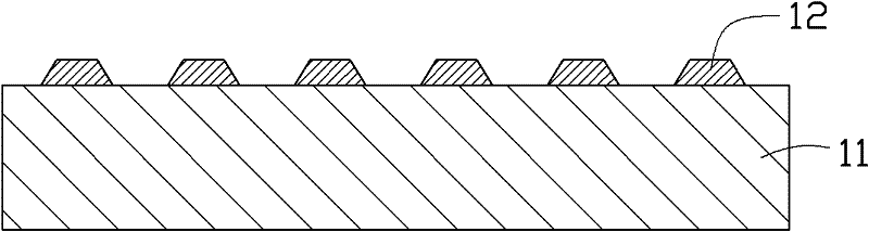
[0049] See figure 1 First, a substrate 11 is provided, and a patterned epitaxial barrier layer 12 is formed on the substrate 11. The substrate 11 can be formed of sapphire, silicon carbide (SiC), silicon (Si) and other materials.
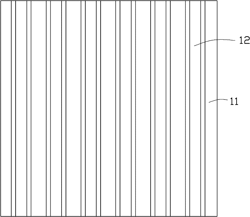
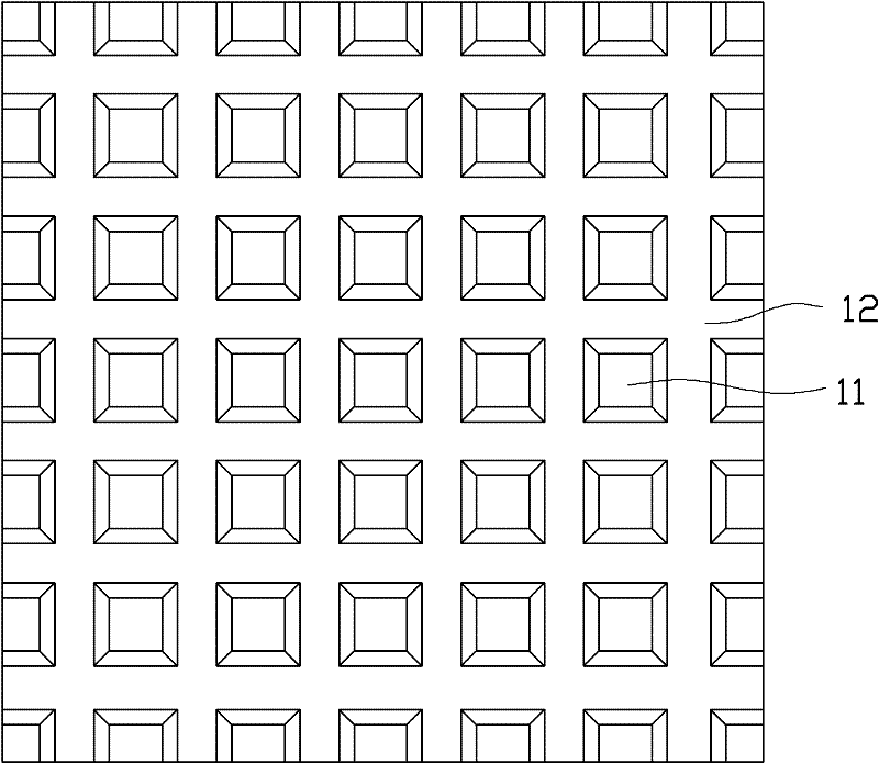
[0050] The patterned epitaxial barrier layer 12 can be a plurality of independent patterns that are not connected to each other, for example figure 2 As shown, the patterned epitaxial barrier layer 12 is composed of a plurality of strip-shaped silicon dioxide layers arranged in parallel. The patterned epitaxial barrier layer 12 can also be a continuous pattern, for example image 3 As shown, the patterned epitaxial barrier layer 12 is composed of striped silicon dioxide layers arranged crosswise to form a grid structure. Of course, the composition and shape of the patterned epitaxial barrier layer 12 can be designed according to needs. The patterned epitaxial barrier layer 12 can be made of silicon dioxide (SiO 2 ), silicon nitride (SiN) and ot...
no. 2 example
[0058] See Figure 11 , fabricate a patterned epitaxial barrier layer 32 on a substrate 31 . See Figure 12 An n-type semiconductor layer 33 is grown on the surface of the substrate 31 having the patterned epitaxial barrier layer 32 , and at this time, the growth of the n-type semiconductor layer 33 is stopped when the n-type semiconductor layer 33 does not completely cover the patterned epitaxial barrier layer 32 . See Figure 13 , using a buffered etchant to remove the patterned epitaxial barrier layer 32 , leaving a hole 41 in its position that matches the shape of the original patterned epitaxial barrier layer 32 . See Figure 14 , continue to grow the n-type semiconductor layer 33 on the substrate 31 until the n-type semiconductor layer 33 becomes a continuous film layer. The above steps are basically the same as those in the first embodiment, and will not be repeated here.
[0059] See Figure 15 , etch the n-type semiconductor layer 33 to a position close to the h...
no. 3 example
[0069] Such as Figure 10 As shown, a light emitting diode grain 10 includes a substrate 11, an n-type semiconductor layer 13 formed on the substrate 11, a hole 21 formed on the interface 109 between the n-type semiconductor layer 13 and the substrate 11, and a hole 21 formed on the n-type semiconductor layer 13 and the substrate 11. The light emitting structure 108 on the semiconductor layer 13 . The holes 21 are distributed in a pattern, and the n-type semiconductor layer 13 completely covers the holes 21 . The light emitting structure 108 is disposed opposite to the patterned hole 21 , and the light emitting structure 108 includes an active layer 14 formed on the n-type semiconductor layer 13 , a p-type semiconductor current blocking layer 15 , and a p-type semiconductor contact layer 16 . A p-type contact electrode 17 is formed on the p-type semiconductor contact layer 16 , and an n-type contact electrode 18 is formed on the n-type semiconductor layer 13 .
[0070] The p...
PUM
 Abstract
Description
Claims
Application Information
 - R&D
- Intellectual Property
- Life Sciences
- Materials
- Tech Scout
- Unparalleled Data Quality
- Higher Quality Content
- 60% Fewer Hallucinations
Browse by: Latest US Patents, China's latest patents, Technical Efficacy Thesaurus, Application Domain, Technology Topic, Popular Technical Reports.
© 2025 PatSnap. All rights reserved.Legal|Privacy policy|Modern Slavery Act Transparency Statement|Sitemap|About US| Contact US: help@patsnap.com