Optical element, light source device, and projection display device
A technology of optical components and light-emitting components, applied in the field of optical components
- Summary
- Abstract
- Description
- Claims
- Application Information
AI Technical Summary
Problems solved by technology
Method used
Image
Examples
no. 1 example
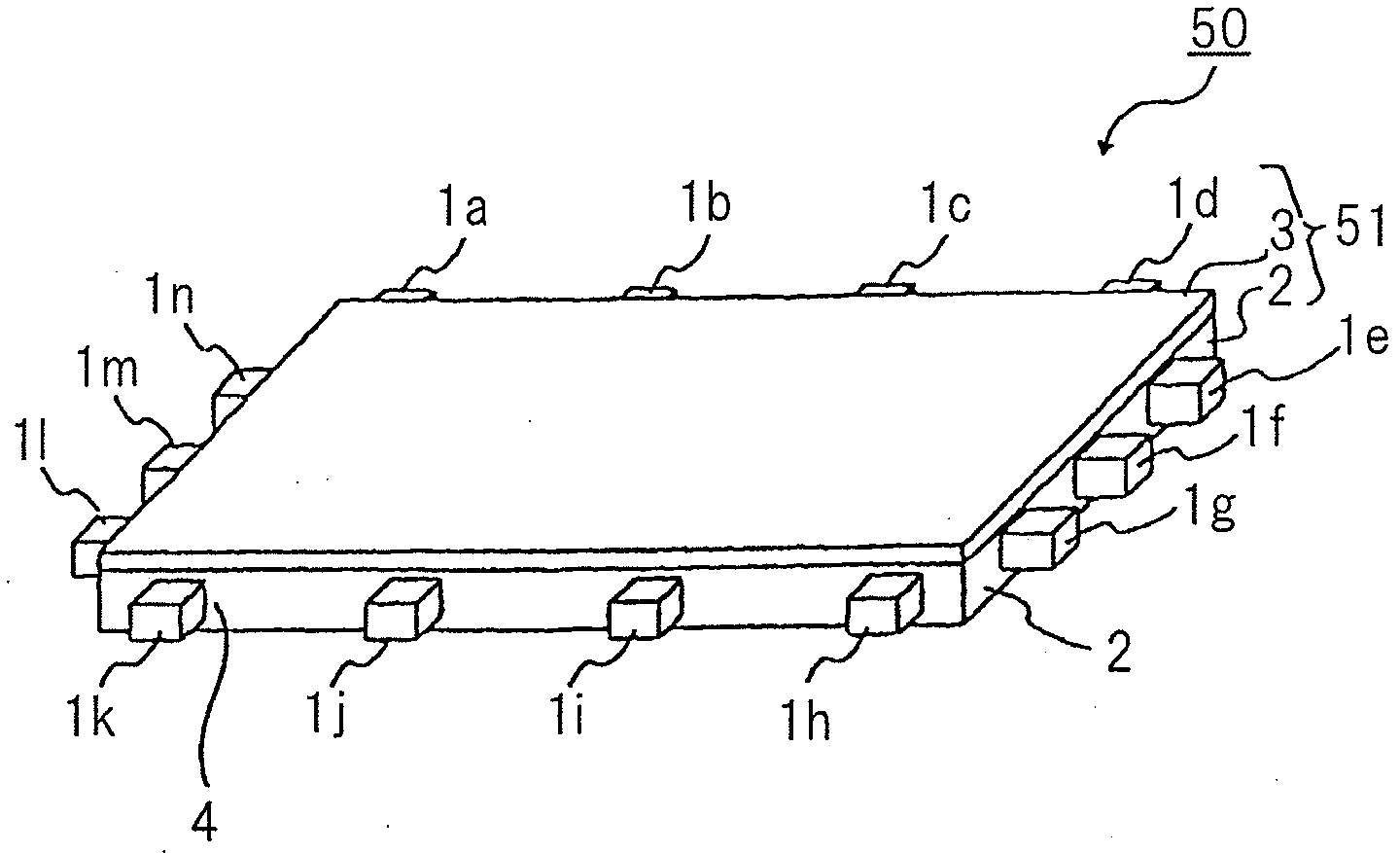
[0072] image 3 is a schematic perspective view showing the configuration of the light source device according to the first embodiment. Figure 4 is an explanatory cross-sectional view showing the behavior of light in the light source device according to the present invention. In the light source device, each layer actually has a very large thickness, and there is a large difference in thickness among the layers. Therefore, it is difficult to draw the various layers with precise scale and scale. Accordingly, in the drawings, the layers are not drawn to scale and are thus shown schematically.
[0073] Such as image 3 and 4 As shown in , a light source device 50 according to this embodiment includes a plurality of light emitting elements 1 (1a to 1n) and an optical element 51 into which light from the light emitting elements 1 is incident. The optical element 51 includes: a light guide body 2 into which the light output from the light emitting element 1 is incident; light...
no. 2 example
[0124] Figure 11 is a perspective view showing the directivity control layer included in the light source device according to the second embodiment. Such as Figure 11 As shown in , in the directivity control layer 18 according to the second embodiment, the carrier generation layer 16, the plasmon excitation layer 8, and the wave vector conversion layer 17 made of photonic crystals are sequentially stacked on the light guiding on body 2.
[0125] In the directivity control layer 18 according to the second embodiment, the wave vector conversion layer 17 also serves as the high dielectric constant layer 9 of the first embodiment, and the carrier generation layer 16 also serves as the low dielectric constant layer 9 of the first embodiment. Dielectric constant layer 7 . Therefore, in order to generate plasmon bonding at the plasmon excitation layer 8, the dielectric constant of the wave vector conversion layer 17 located adjacent to the exit-side interface of the plasmon exci...
no. 3 example
[0128] Figure 12 is a perspective view showing the directivity control layer included in the light source device according to the third embodiment. Such as Figure 12 As shown in , in the directivity control layer 19 according to the third embodiment, the carrier generation layer 6, the low dielectric constant layer 7, the plasmon excitation layer 8, and the wave vector conversion layer made of photonic crystal Layers 17 are stacked successively on the light guide 2 .
[0129] In the directivity control layer 19 according to the third embodiment, the wave vector conversion layer 17 also serves as the high dielectric constant layer 9 of the first embodiment. Therefore, in order to generate plasmon coupling at plasmon excitation layer 8 , the dielectric constant of wave vector conversion layer 17 is set higher than that of low dielectric constant layer 7 . However, even when the dielectric constant of wave vector conversion layer 17 is lower than that of low dielectric const...
PUM
 Abstract
Description
Claims
Application Information
 - R&D
- Intellectual Property
- Life Sciences
- Materials
- Tech Scout
- Unparalleled Data Quality
- Higher Quality Content
- 60% Fewer Hallucinations
Browse by: Latest US Patents, China's latest patents, Technical Efficacy Thesaurus, Application Domain, Technology Topic, Popular Technical Reports.
© 2025 PatSnap. All rights reserved.Legal|Privacy policy|Modern Slavery Act Transparency Statement|Sitemap|About US| Contact US: help@patsnap.com


