SMD (surface mounted device) with cooling and electromagnetic wave absorption functions and preparation method and application thereof

An electromagnetic wave and electromagnetic wave absorption technology, applied in chemical instruments and methods, lamination auxiliary operations, special decorative structures, etc., can solve the problems of aggravating internal heat dissipation of electronic products, unfavorable heat transfer to the outside of equipment, and low thermal conductivity of ferrite , to improve the comfort of the human body, reduce the temperature of the components, and improve the reliability of the equipment

Inactive Publication Date: 2012-07-11
深圳市爱诺菲科技有限公司
View PDF7 Cites 33 Cited by
  • Summary
  • Abstract
  • Description
  • Claims
  • Application Information

AI Technical Summary

Problems solved by technology

[0004] In the existing mobile phone radiation protection technology, for example, gaskets containing ferrite or wave absorbers are pasted on the surface of the chip or inside the circuit board and the casing, so that the electromagnetic wave is partially controlled, because the wave absorbing material converts the electromagnetic energy in...

Method used


Image

  • SMD (surface mounted device) with cooling and electromagnetic wave absorption functions and preparation method and application thereof
  • SMD (surface mounted device) with cooling and electromagnetic wave absorption functions and preparation method and application thereof
  • SMD (surface mounted device) with cooling and electromagnetic wave absorption functions and preparation method and application thereof

Examples


Embodiment 1

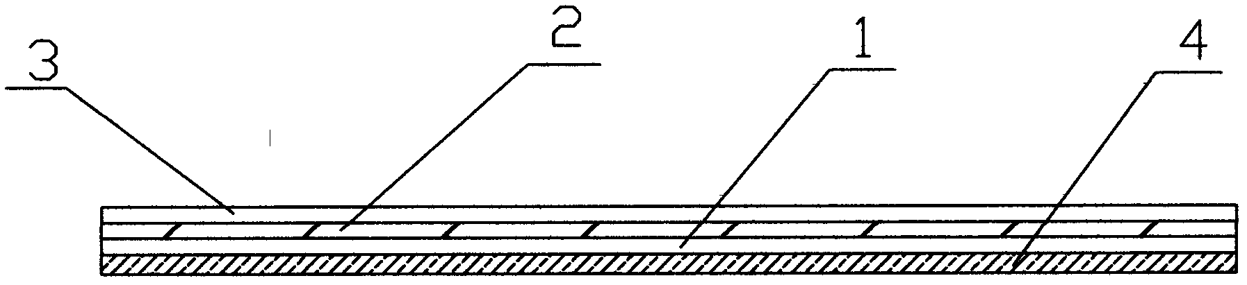
[0063] Such as figure 1 As shown, the heat dissipation electromagnetic wave absorbing patch described in the application of the present invention includes a decorative layer 3, a heat dissipation wave absorbing layer 2 and a bonding layer 1 for heat dissipation and absorbing electromagnetic waves, and the heat dissipation wave absorbing layer 2 is located on the decoration layer 3 and bonded Between the layers 1, further, the heat dissipation electromagnetic wave absorption patch also includes a protective peeling layer 4, and the protective peeling layer 4 is located under the bonding layer 1 to protect the stickiness of the bonding layer 1. Before peeling off the protective peeling layer 4, the patch is attached to the position where heat dissipation and electromagnetic wave absorption are required. The decorative layer 3 is made of printable single-sided self-adhesive polyester film, with a thickness of 0.025mm, and the surface is printed with decorative patterns; the heat ...

Embodiment 2

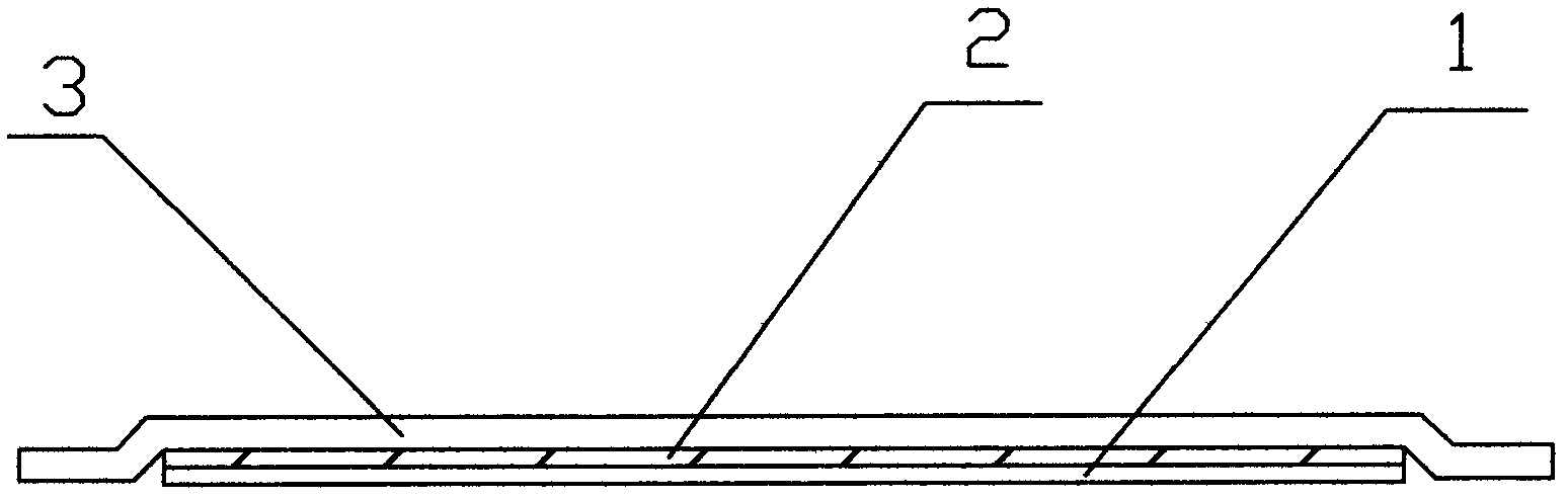
[0065] Such as figure 2 , in this embodiment, from bottom to top, followed by bonding layer 1, heat radiation absorbing layer 2 and decorative layer 3, each layer is a single-layer structure, and the area of ​​decorative layer 3 is larger than the bonding layer 1 and heat dissipation layer The area of ​​the wave-absorbing layer 2 completely covers the heat-dissipating wave-absorbing layer 2 and the bonding layer 1 from above.

Embodiment 3

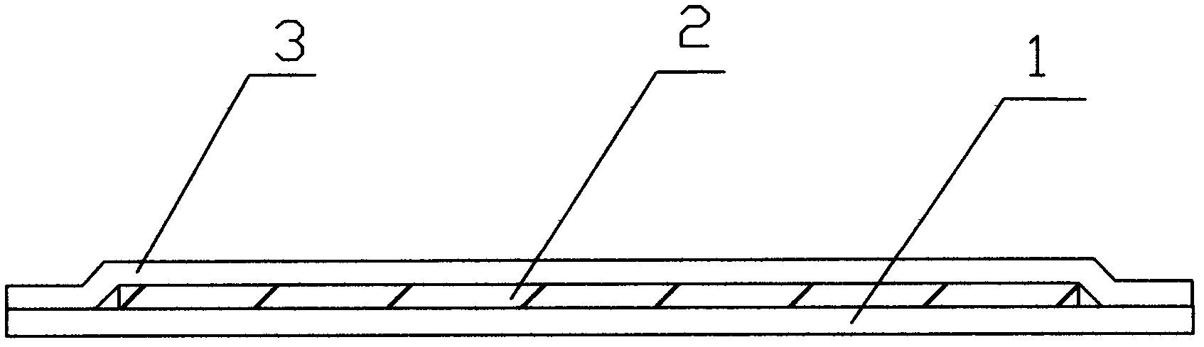
[0067] Such as image 3 , in this embodiment, from bottom to top, there are bonding layer 1, heat radiation absorbing layer 2 and decorative layer 3, each layer is a single-layer structure, and the area of ​​decorative layer 3 and bonding layer 1 is larger than the heat dissipation layer The area of ​​the wave-absorbing layer 2 completely covers the heat-dissipating wave-absorbing layer 2 from above and below.


PUM

PropertyMeasurementUnit
Thicknessaaaaaaaaaa
Plane thermal conductivityaaaaaaaaaa
Thicknessaaaaaaaaaa

Abstract

Aiming at the problems existing in the present cooling and radiation protection technologies of electronic products, the invention provides an SMD (surface mounted device) with cooling and electromagnetic wave absorption functions, which is applied to electronic equipment. The SMD comprises a decoration layer, a cooling and electromagnetic wave absorption layer for cooling and electromagnetic wave absorption and a mounting layer, wherein the cooling and electromagnetic wave absorption layer is arranged between the decoration layer and the mounting layer. The SMD further comprises a protective stripping layer which is arranged below the mounting layer and used for protecting the adhesiveness of the mounting layer, and the stripping layer is taken off before the SMD is used, and then the SMD is mounted at a position needing cooling and electromagnetic wave absorption. Furthermore, the cooling and electromagnetic wave absorption layer is of a structure consisting of more than two layers, including a cooling layer and an electromagnetic wave absorption layer which are independent from each other; accordingly, the cooling and electromagnetic wave absorption layer can be a single-layer structure and is made of a material with cooling and cooling and electromagnetic wave absorption functions. The invention also provides the preparation and application methods of the SMD. The SMD with cooling and electromagnetic wave absorption functions is applied to a shell of electronic equipment, and the shell of the electronic equipment includes but is not limited to a mobile phone shell, a network card, a panel personal computer shell hot spot, a netbook shell hot spot, notebook computer shell hot spot, game equipment and other consumer mobile equipment can improve cooling effect, reduce temperature and weaken electromagnetic wave radiation.

Description

technical field [0001] The application of the present invention relates to a heat dissipation electromagnetic wave absorption patch for electronic equipment and its manufacturing method and application, belonging to the technical field of heat dissipation equipment for electronic products. Background technique [0002] With the rapid development of consumer electronic products, high-performance ultra-thin electronic equipment represented by mobile phones and tablet computers, and large-screen touch electronic equipment are becoming more and more popular, which brings CPU, power chips, radio frequency chips and other components The calorific value is obviously increased, and the problem of electromagnetic radiation is also becoming more and more prominent. In order to meet the needs of the market, consumer electronics products are developing towards smaller sizes and thinner designs. The popularization of 3G, 4G mobile phones, tablet computers, e-books, notebook computers and...

Claims


Application Information

Patent Timeline
IPC IPC(8): B32B5/00B32B38/04B32B38/10B44C5/04H05K7/20
Inventor 杜明亮杜明卫杜明风
Owner 深圳市爱诺菲科技有限公司
Why Eureka
Try Eureka