Method for manufacturing vertically interconnecting carbon nanotube bundle

A technology of carbon nanotube bundles and manufacturing methods, which is applied in the field of three-dimensional stacking, can solve problems such as process incompatibility, inapplicability of carbon nanotube bundles, and difficult implementation of mature processes, so as to improve interconnection reliability and performance, and improve interconnection. Reliability and performance, the effect of mature and easy process

Active Publication Date: 2012-07-11
NAT CENT FOR ADVANCED PACKAGING
View PDF4 Cites 15 Cited by
  • Summary
  • Abstract
  • Description
  • Claims
  • Application Information

AI Technical Summary

Problems solved by technology

However, this method is not suitable for the production of carbon nanotube bundles in silicon-based TSV. At the same time, this method is not only incompatible with the TSV process, but also the process is mature and difficult to implement.

Method used


Image

  • Method for manufacturing vertically interconnecting carbon nanotube bundle
  • Method for manufacturing vertically interconnecting carbon nanotube bundle
  • Method for manufacturing vertically interconnecting carbon nanotube bundle

Examples


Embodiment 1

[0060] The specific process steps are as follows:

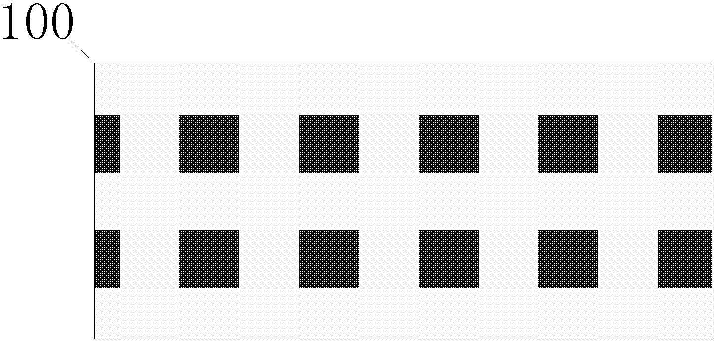
[0061] Step 01, such as figure 1 As shown, in the silicon substrate used for making carbon nanotube bundles provided in this embodiment, a 4-inch silicon wafer is selected as the upper end 100 of the silicon substrate, and the thickness of the bottom of the silicon substrate is 500 microns.

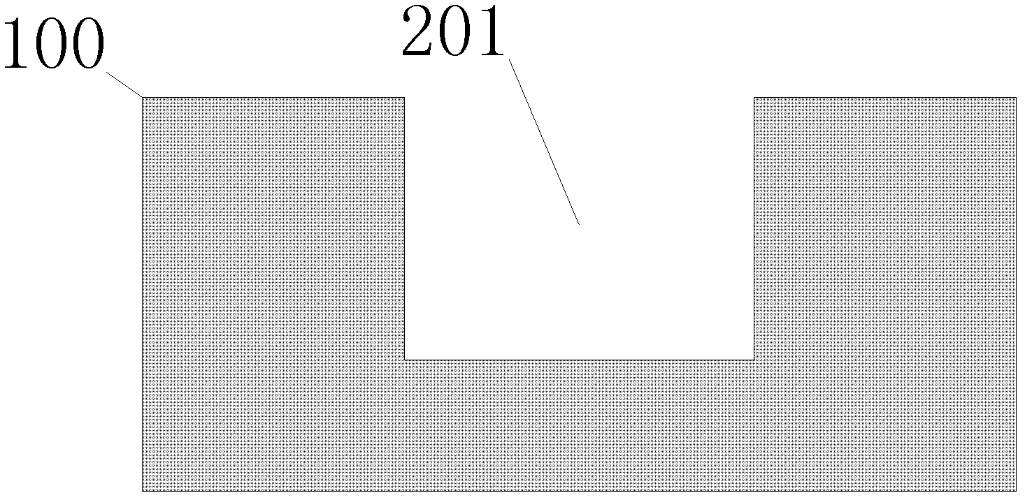
[0062] Step 02, using DRIE (Deep Reactive Ion Etching) method to make TSV blind holes 201, such as figure 1 As shown, a TSV blind via is fabricated on the silicon substrate provided in this embodiment, the size of the hole is 10 microns, and the depth of the hole is 50 microns.

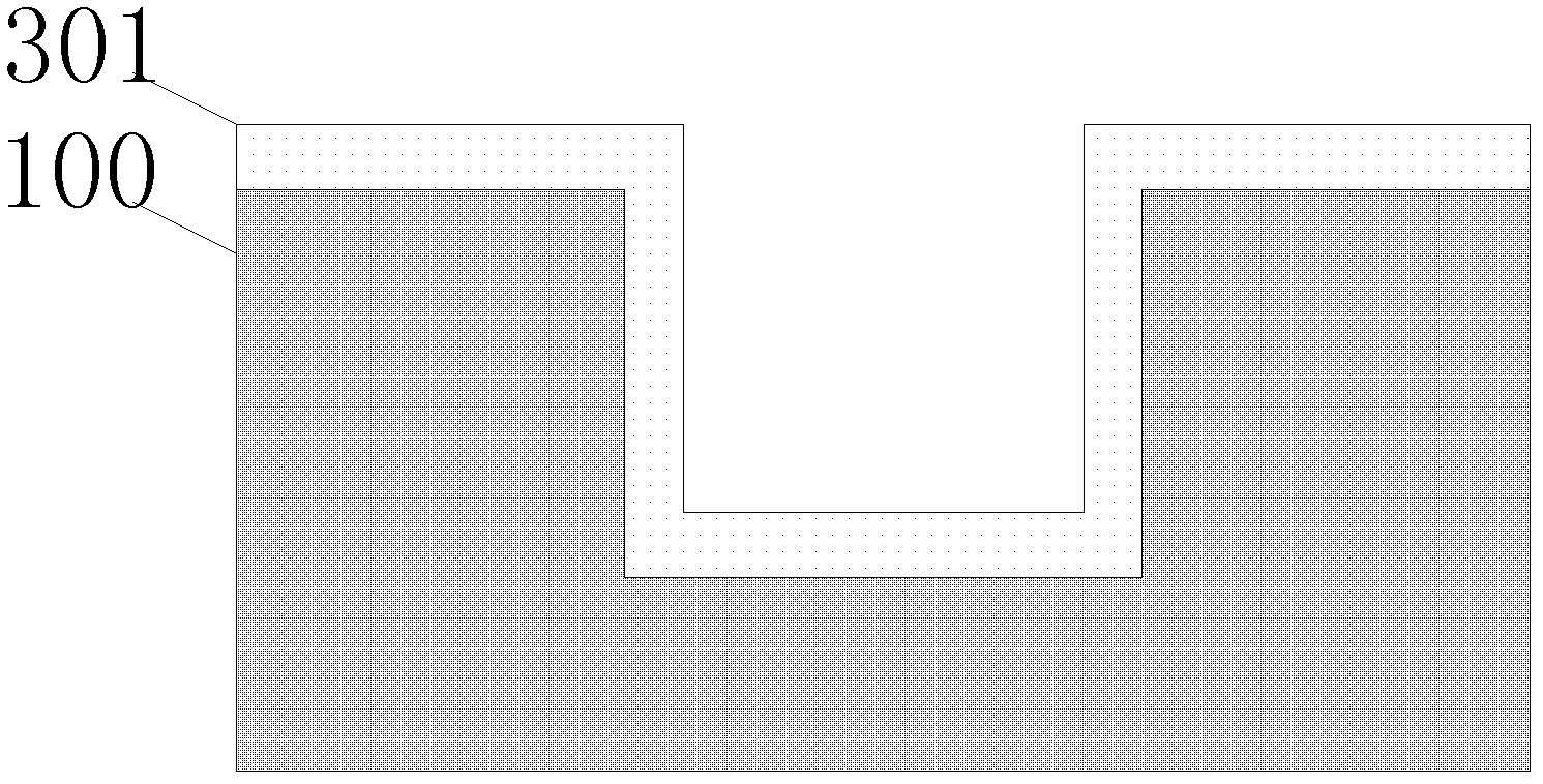
[0063] Step 03, using a thermal oxidation method to make a silicon dioxide insulating layer, such as image 3 As shown, in this embodiment, an insulating layer 301 and a barrier layer are formed in the TSV blind hole and on the upper end of the silicon substrate. The thickness of the insulating layer is 1 micron, and titanium nitride is formed on the insulatin...


PUM

PropertyMeasurementUnit
thicknessaaaaaaaaaa
thicknessaaaaaaaaaa

Abstract

The invention discloses a method for manufacturing a vertically interconnecting carbon nanotube bundle with high interconnecting reliability and high performance. The method is compatible with a through silicon via (TSV) process and is mature and easy to implement. The method comprises the following steps of: forming a hole, and depositing a metal catalyst film at the bottom of the TSV only, so that the carbon nanotube bundle vertically grows at the bottom of the TSV from bottom to top so as to fill the TSV. Meanwhile, gas between carbon nanotubes is exhausted through densification operation so as to improve the density of the carbon nanotube bundle; and an interconnecting structure of the metal-coated carbon nanotube bundle is manufactured, and the interconnecting reliability and the performance of the carbon nanotube bundle can be effectively improved by taking the interconnecting structure as an interconnecting material. The invention has the advantages that: the method is compatible with the TSV process and is mature and easy to implement, and the interconnecting reliability and the performance can be greatly improved.

Description

technical field [0001] The invention relates to the technical field of three-dimensional stacking in chip packaging technology, and in particular to a method for manufacturing vertical interconnection of carbon nanotube bundles. Background technique [0002] In recent years, advanced packaging technology has begun to appear in the IC manufacturing industry, especially three-dimensional (3D) packaging first breaks through the traditional concept of planar packaging, and the assembly efficiency is as high as 200%. It allows multiple chips to be stacked in a single package to double the storage capacity, which is called a stacked 3D package in the industry; secondly, it directly interconnects the chips, the length of the interconnection line is significantly shortened, and the signal transmission is faster and more efficient. The interference is less; moreover, it stacks multiple chips with different functions together, so that a single package can achieve more functions, thus ...

Claims


Application Information

Patent Timeline
Patent Type & Authority Applications(China)
IPC IPC(8): H01L21/768
Inventor 曹立强戴风伟周静刘丰满潘茂云
Owner NAT CENT FOR ADVANCED PACKAGING
Why Eureka
Try Eureka