Thin film transistor and manufacturing method for same, semiconductor device and manufacturing method for same, and display device

A technology of thin-film transistors and manufacturing methods, which is applied in semiconductor/solid-state device manufacturing, transistors, semiconductor devices, etc., and can solve problems such as opening contact holes at the same time

Inactive Publication Date: 2012-07-11
SHARP KK
View PDF5 Cites 11 Cited by
  • Summary
  • Abstract
  • Description
  • Claims
  • Application Information

AI Technical Summary

Problems solved by technology

Therefore, it is difficult to open the contact holes on the source region and the drain region in the same process as the contact holes on the gate electrode. In the prior art, these contact holes are respectively opened in different processes.

Method used


Image

  • Thin film transistor and manufacturing method for same, semiconductor device and manufacturing method for same, and display device
  • Thin film transistor and manufacturing method for same, semiconductor device and manufacturing method for same, and display device
  • Thin film transistor and manufacturing method for same, semiconductor device and manufacturing method for same, and display device

Examples


no. 1 approach

[0119]

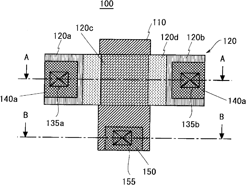
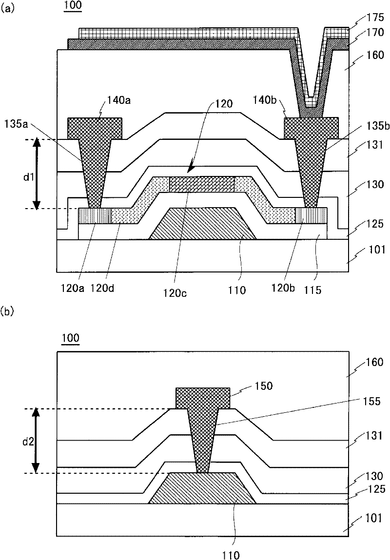
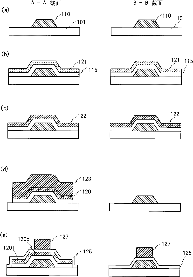
[0120] figure 1 is a plan view showing the structure of TFT 100 according to the first embodiment of the present invention, figure 2 (a) is based on figure 1 A cross-sectional view of the TFT 100 cut along the line A-A shown, figure 2 (b) is based on figure 1 A cross-sectional view of the TFT 100 cut along the line B-B shown. in addition, figure 1 In FIG. 2 , illustrations of insulating films such as gate insulating films, interlayer insulating films, and planarizing films are omitted for easier understanding. In addition, the TFT 100 is a TFT used as a switching element provided in a pixel forming portion of a liquid crystal display device.

[0121] refer to figure 1 and figure 2 The structure of TFT100 is demonstrated. like figure 1 and figure 2 As shown, a gate electrode 110 containing metal is formed on a glass substrate 101 which is an insulating substrate. A gate insulating film 115 is formed to cover a part of the surface of the gate elec...

no. 2 approach

[0143]

[0144] A plan view of TFT 200 of the second embodiment and figure 1 Since the top view of the TFT 100 of the first embodiment shown is the same, description thereof is omitted. Figure 5 (a) is based on figure 1 A cross-sectional view of the TFT 200 cut along the same cross-section as the line A-A shown, Figure 5 (b) is based on figure 1 A cross-sectional view of the TFT 200 cut along the same cross-section as the line B-B shown. In addition, in Figure 5 (a) and Figure 5 (b), for figure 2 (a) and figure 2 The same constituent elements as the constituent elements of the TFT 100 shown in (b) are denoted by the same reference numerals, and description thereof will be omitted.

[0145] like Figure 5 (a) and Figure 5 As shown in (b), unlike the case of TFT100, in TFT200, protective film 226 is further formed on the surface of gap film 125 formed on source region 120a and drain region 120b. However, if Figure 5 As shown in (b), on the gate contact re...

no. 3 approach

[0161]

[0162] In this embodiment, a description will be given of a semiconductor device 300 in which a TFT 301 having a bottom gate structure and a photodiode 302 having a light-shielding film are formed on the same glass substrate 101 . Figure 8 is a plan view showing the structure of a semiconductor device 300 according to a third embodiment of the present invention, Figure 9 (a) is based on Figure 8 A cross-sectional view of the TFT301 cut off by the line C-C shown, Figure 9 (b) is based on Figure 8 A cross-sectional view of the TFT301 cut by the line D-D shown, Figure 9 (c) is based on Figure 8 A cross-sectional view of photodiode 302 is shown cut through line E-E. In addition, in Figure 8 In FIG. 2 , illustrations of insulating films such as a gate insulating film, an interlayer insulating film, and a planarizing film are omitted for clarity.

[0163] The TFT 301 of the bottom gate structure included in the semiconductor device 300, and figure 1 and ...


PUM

PropertyMeasurementUnit
thicknessaaaaaaaaaa

Abstract

Disclosed is a thin film transistor manufacturing method in which the process for opening contact holes has been simplified. Due to the removal in advance of a gate insulating film (115) which is formed on a gate electrode (110) not covered by a channel layer (120) of a TFT (100), the film thickness of the insulating film formed on the gate electrode (110) which is not covered by the channel layer (120) is the same as the film thickness of the insulating film formed on the source region (120a) and the drain region (120b). Therefore, it is possible to simultaneously open a contact hole (155) which reaches the surface of the gate electrode (110), a contact hole (135a) which reaches the surface of the source region (120a), and a contact hole (135b) which reaches the surface of the drain region (120b).

Description

technical field [0001] The present invention relates to a thin film transistor, a manufacturing method thereof, a semiconductor device, a manufacturing method thereof, and a display device, and more specifically, a bottom-gate thin film transistor, a manufacturing method thereof, a semiconductor device, a manufacturing method thereof, and a display device. Background technique [0002] In the manufacturing process of a thin film transistor (Thin Film Transistor, hereinafter referred to as "TFT") with a bottom gate structure, contact holes are opened in the source region and the drain region for electrical connection with the source electrode and the drain electrode, respectively. Next, it is necessary to etch an insulating film called a gap film and an interlayer insulating film formed on the surface of the gap film. On the other hand, on the surface of the gate electrode not covered by the channel layer, a gate insulating film, a gap film, and an interlayer insulating layer...

Claims


Application Information

Patent Timeline
Patent Type & Authority Applications(China)
IPC IPC(8): H01L29/786H01L21/768H01L27/146G02F1/136G02F1/1368H01L21/28H01L21/336
CPCH01L29/78621H01L27/1214H01L29/66765G02F1/136227H01L29/41733H01L27/124H01L27/1248
Inventor 富安一秀北角英人宫本忠芳
Owner SHARP KK
Why Eureka
Try Eureka