Electrode of p-type gallium nitride-based device as well as preparation method and application thereof
A gallium nitride-based and gallium nitride technology, which is applied to the electrode of p-type gallium nitride-based device and its preparation field, can solve the problems of increasing the height of the Schottky barrier, and solve the problem of increasing the height of the Schottky barrier. High, improve performance, reduce the effect of ohmic contact resistance
- Summary
- Abstract
- Description
- Claims
- Application Information
AI Technical Summary
Problems solved by technology
Method used
Image

Examples
Embodiment 1
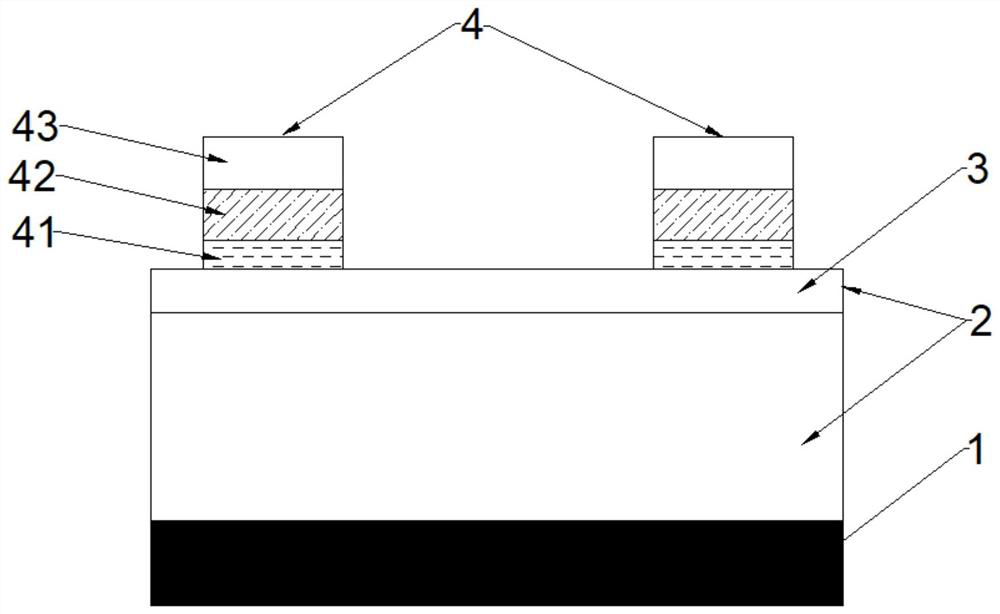
[0052] Such as figure 1 As shown: this embodiment provides an electrode 4 of a p-type GaN-based device, the electrode 4 includes a nickel oxide layer 41, a platinum layer 42 and a gold layer 43 stacked in sequence, wherein the nickel oxide layer 41 It is a p-type structure, the platinum layer 42 is located in the middle of the nickel oxide layer 41 and the gold layer 43, the nickel oxide layer 41 is an ohmic contact layer of a p-type gallium nitride-based device, and the electrode is used for the device source and drain.
[0053] Wherein, the total thickness of the source electrode is 115nm, the thickness of the nickel oxide layer 41 is 10nm, the thickness of the platinum layer 42 is 30nm, and the thickness of the gold layer 43 is 75nm;
[0054] The total thickness of the drain electrode is 115 nm, the thickness of the nickel oxide layer 41 is 10 nm, the thickness of the platinum layer 42 is 30 nm, and the thickness of the gold layer 43 is 75 nm.
[0055] The preparation met...
Embodiment 2
[0062] The difference between this embodiment and Embodiment 1 is that in this embodiment, the electrodes are etched, a pit is formed in the electrode area, and then metal is deposited on the pit.
[0063] The preparation method of described electrode is as follows:
[0064] (1) Deposit a layer of 100nm thick silicon oxide on the p-type gallium nitride epitaxial structure as a hard mask, and spin-coat a layer of photoresist on the p-type gallium nitride included in the p-type gallium nitride epitaxial structure , and then after exposure and development, the source and drain regions of the p-type GaN-based device are exposed;
[0065] (2) Remove the silicon oxide covering the source and drain regions by ICP dry etching, then rinse the sample in step (1) with deionized water for 3 minutes, and finally dry it with nitrogen to clean off the photoresist;
[0066] (3) Soak the sample treated in step (2) in BEO for 3 minutes, then rinse with deionized water for 3 minutes, and blow d...
Embodiment 3
[0071] The difference between the electrode provided in this embodiment and Embodiment 2 is that, after the electrode is patterned, it will appear as etching holes distributed in a matrix with intervals in the electrode area.
[0072] The difference between this embodiment and embodiment 2 also includes, between step (2) and step (3), adding a step, the added step is:
[0073] After cleaning in step (2), spin-coat a layer of photoresist on the source and drain regions, and then expose and develop, so that the source and drain regions have multiple rectangles;
[0074] All the other preparation methods and parameters are consistent with Example 2.
PUM
| Property | Measurement | Unit |
|---|---|---|
| Thickness | aaaaa | aaaaa |
| Thickness | aaaaa | aaaaa |
| Thickness | aaaaa | aaaaa |
Abstract
Description
Claims
Application Information
 - R&D
- Intellectual Property
- Life Sciences
- Materials
- Tech Scout
- Unparalleled Data Quality
- Higher Quality Content
- 60% Fewer Hallucinations
Browse by: Latest US Patents, China's latest patents, Technical Efficacy Thesaurus, Application Domain, Technology Topic, Popular Technical Reports.
© 2025 PatSnap. All rights reserved.Legal|Privacy policy|Modern Slavery Act Transparency Statement|Sitemap|About US| Contact US: help@patsnap.com