A method of forming micro-pattern in semiconductor device

A micro-pattern and semiconductor technology, applied in the field of semiconductor manufacturing and semiconductor integrated circuit manufacturing, can solve the problems of complex process operation and cannot be widely used, and achieve the effect of simple operation process, improved overlay accuracy, and improved product yield.

Pending Publication Date: 2020-03-24
CHANGXIN MEMORY TECH INC
View PDF2 Cites 0 Cited by
  • Summary
  • Abstract
  • Description
  • Claims
  • Application Information

AI Technical Summary

Problems solved by technology

[0009] The above methods are complicated to operate and cannot be popularized and used on a large scale

Method used


Image

  • A method of forming micro-pattern in semiconductor device
  • A method of forming micro-pattern in semiconductor device
  • A method of forming micro-pattern in semiconductor device

Examples


Embodiment Construction

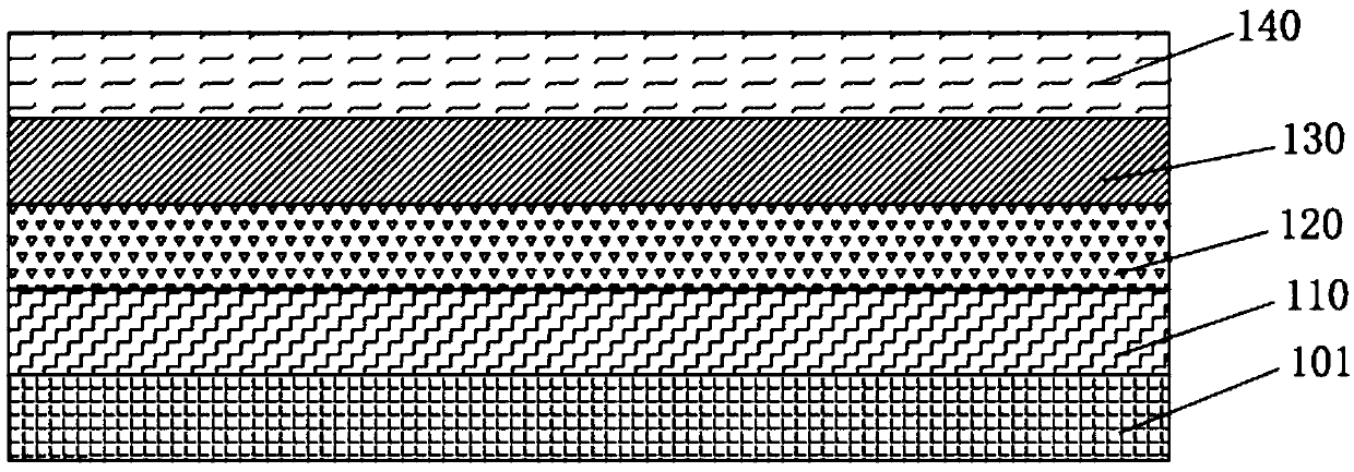
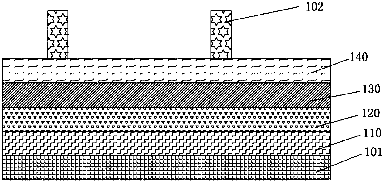
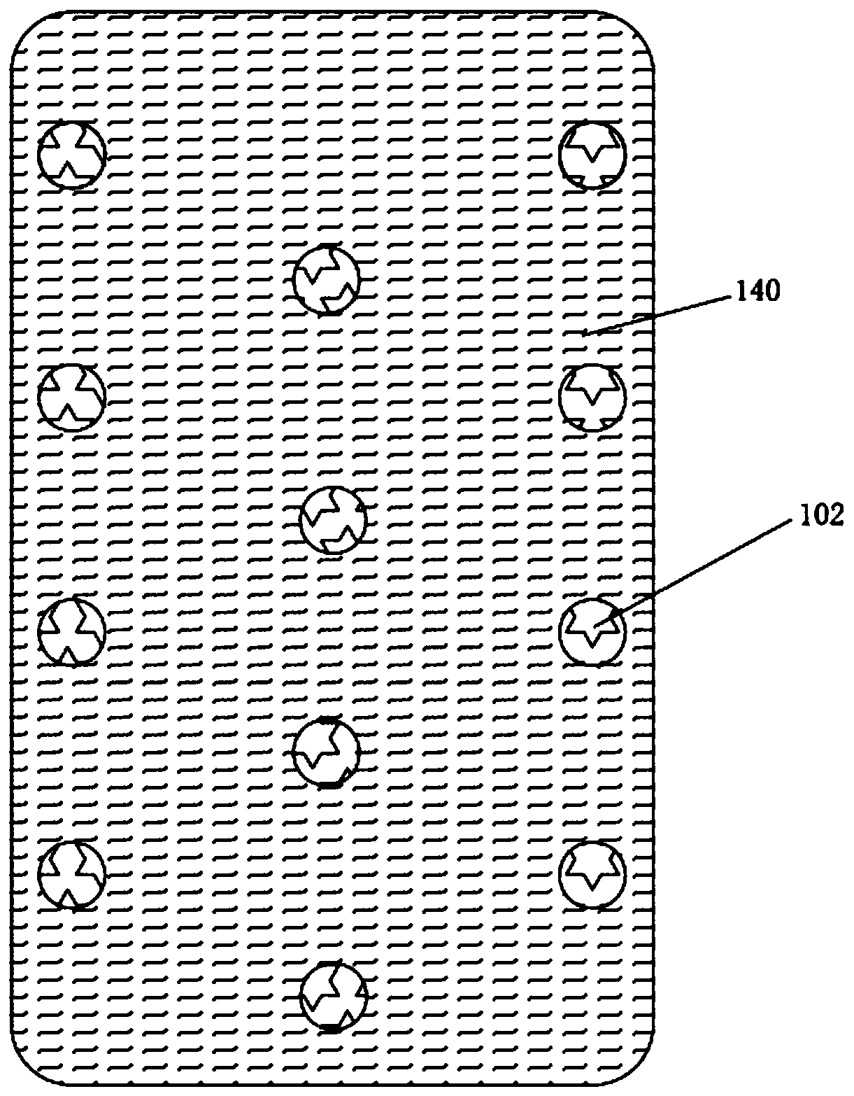
[0054] In order to make the purpose and technical solutions of the embodiments of the present invention more clear, the technical solutions of the present invention will be clearly and completely described below in conjunction with the embodiments of the present invention. Apparently, the described embodiments are some, not all, embodiments of the present invention. Based on the described embodiments of the present invention, all other embodiments obtained by persons of ordinary skill in the art without creative efforts shall fall within the protection scope of the present invention.

[0055] Those skilled in the art can understand that, unless otherwise defined, all terms (including technical and scientific terms) used herein have the same meaning as commonly understood by one of ordinary skill in the art to which this invention belongs. It should also be understood that terms such as those defined in commonly used dictionaries should be understood to have a meaning consisten...


PUM


Abstract

The invention provides a method for forming a micro-pattern in a semiconductor device. The method comprises the following steps: providing a substrate, forming a hard mask layer on the substrate, forming a first sacrificial layer on the hard mask layer, forming a second sacrificial layer on the first sacrificial layer, and forming a third sacrificial layer on the second sacrificial layer; firstly,forming a first dot pattern; forming a second dot pattern; forming a third dot pattern; and finally, etching the first sacrificial layer to form a micro-pattern. According to the method, the overlayprecision in the capacitor pattern manufacturing process is improved, the problems of contact resistance and parasitic capacitance are avoided, the product yield is greatly improved, and meanwhile themethod is simple in operation process, low in cost and short in period.

Description

technical field [0001] The invention relates to the field of semiconductor manufacturing, in particular to the field of semiconductor integrated circuit manufacturing, in particular to a method for forming micropatterns in semiconductor devices. Background technique [0002] Photolithography is the fundamental process used in the manufacture of integrated circuits. In general, photolithography involves forming a layer of light or radiation sensitive material, such as a photoresist, over a layer of material or substrate. The radiation sensitive material is selectively exposed to light generated by a light source, such as a deep ultraviolet or extreme ultraviolet source, to transfer the pattern defined by the mask to the radiation sensitive material. The exposed layer of radiation sensitive material is developed to define a patterned mask layer. Then, various process operations, such as etching or ion implantation processes, can be performed on the underlying material layer ...

Claims


Application Information

Patent Timeline
Patent Type & Authority Applications(China)
IPC IPC(8): H01L21/033
CPCH01L21/0337H01L21/0338
Inventor 高玮
Owner CHANGXIN MEMORY TECH INC
Why Eureka
Try Eureka