
Electric field modulation type random memory cell array and memory

A memory cell array and memory cell technology, which is applied in the direction of static memory, digital memory information, electrical components, etc., can solve the problem that the random memory cannot be industrialized, and achieve less manufacturing processes, long service life of the device, and reduce power consumption of the device Effect

Active Publication Date: 2012-07-18
INST OF PHYSICS - CHINESE ACAD OF SCI
View PDF5 Cites 8 Cited by
  • Summary
  • Abstract
  • Description
  • Claims
  • Application Information

AI Technical Summary

Problems solved by technology

However, due to some problems in itself, the above-mentioned random access memory cannot realize large-scale industrialization at present.

Method used

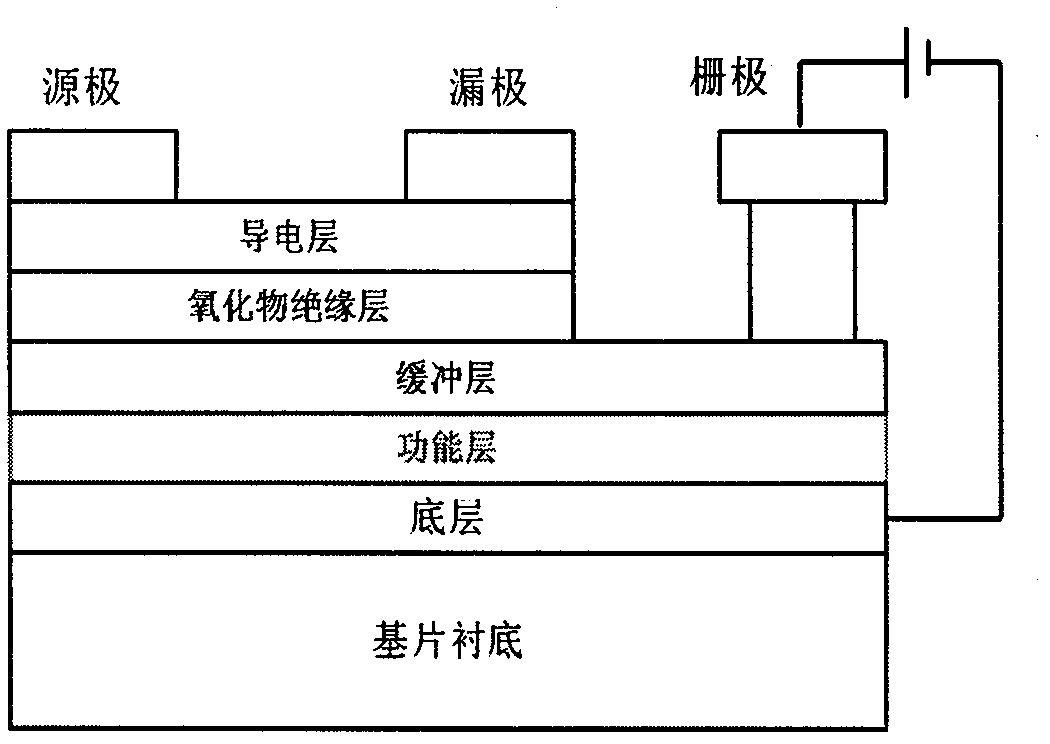
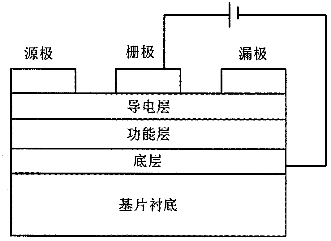
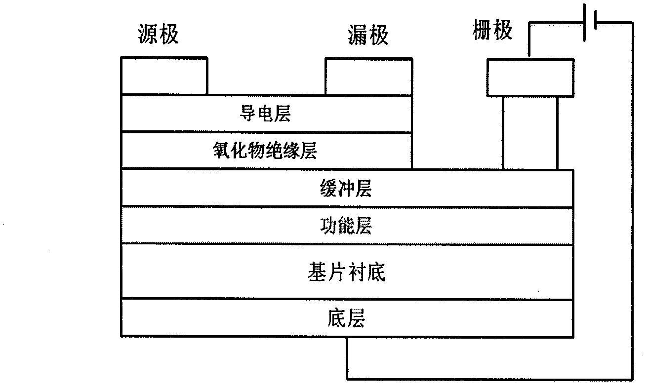

Image

  • Electric field modulation type random memory cell array and memory
  • Electric field modulation type random memory cell array and memory
  • Electric field modulation type random memory cell array and memory

Examples


Embodiment 1

[0066] The present invention provides another new array of electric field modulation memory cells. Figure 2A ( Figure 2A1 , Figure 2A2 , Figure 2A3 ) exemplarily provides a schematic structural diagram of the array unit.

[0067] The conductive layer in the multilayer film in the unit is connected to 2a and 2b through 1a and 1b. The buffer layer is connected to 2c through 1c. The bottom layer is connected by 1d and 2d.

[0068] The multilayer films in the unit are connected through 1a, 1b, 1c and 1d and 2a, 2b, 2c and 2d respectively. 2a and 2d are metal wires for connecting all memory units. 2a and 2d are on the same layer and parallel to each other. 2b and 2c are transition metal layers.

[0069] The electrodes of the transition metal layers 2b and 2c are respectively connected to the wires 4a and 4b through the via holes 3a and 3b. Among them, 4a and 4b are metal wires for connecting all memory cells. 4a and 4b are in the same layer and parallel to each other. ...

Embodiment 2

[0076] The invention provides a novel array of electric field modulation memory cells. Figure 2B ( Figure 2B1 , Figure 2B2 , Figure 2B3 ) exemplarily provides a schematic structural diagram of the array unit.

[0077] The conductive layer in the multilayer film in the unit is connected to 2a, 2b and 2c through 1a, 1b and 1c. The bottom layer is connected by 1d and 2d. 2a and 2d are metal wires for connecting all memory units. 2a and 2d are on the same layer and parallel to each other. 2b and 2c are transition metal layers.

[0078] The electrodes of the transition metal layers 2b and 2c are respectively connected to the wires 4a and 4b through the via holes 3a and 3b. Among them, 4a and 4b are metal wires for connecting all memory cells. 4a and 4b are on the same layer and parallel to each other.

[0079] The wires 2a and 4b are perpendicular to each other and are used to read data from the intersecting units.

[0080] When the 2a and 4b wires are used to read dat...

Embodiment 3

[0085] The present invention provides another new array of electric field modulation memory cells. Figure 2C ( Figure 2C1 , Figure 2C2 , Figure 2C3 ) exemplarily provides a schematic structural diagram of the array unit.

[0086] The conductive layer in the multilayer film in the unit is connected to 2a and 2b through 1a and 1b. The buffer layer is connected to 2c through 1c. The bottom layer on the backside of the substrate is connected by 1d and 2d.

[0087] The multilayer films in the unit are connected through 1a, 1b, 1c and 1d and 2a, 2b, 2c and 2d respectively. 2a and 2d are metal wires for connecting all memory units. 2a and 2d are on the same layer and parallel to each other. 2b and 2c are transition metal layers.

[0088] The electrodes of the transition metal layers 2b and 2c are respectively connected to the wires 4a and 4b through the via holes 3a and 3b. Among them, 4a and 4b are metal wires for connecting all memory cells. 4a and 4b are in the same l...


PUM

PropertyMeasurementUnit
Thicknessaaaaaaaaaa
Thicknessaaaaaaaaaa
Thicknessaaaaaaaaaa

Abstract

Disclosed are a novel electric field modulation type memory cell array and a random memory, wherein the memory comprises the novel electric field modulation type memory cell array and a corresponding read-write circuit. The memory cells in the memory cell array can use a structure of conducting layers, function layers and base layers or a structure of conducting layers, insulation layers, buffer layers, function layers and base layers. Both the structures are provided with two data reading lines and two data writing lines. The memory cells in the novel electric field modulation type memory cell array also can use a structure combined with a transistor and utilize the transistor to select memory cells. The random memory comprises a decoder of elementary rows, a sense amplifier, a decoder of columns, a register, a control circuit, a read-write driver, an input interface, an output interface and the like. The novel random memory has the advantages of being simple in structure, long in service life of components, low in power consumption and the like.

Description

technical field [0001] The invention relates to the technical field of an electric field modulation random access memory, in particular, the invention relates to an electric field modulation random access memory unit array and an electric field modulation random access memory. Background technique [0002] Dynamic random access memory (DRAM) is an important part of current computers, and is often called memory. The DRAM cell structure is very simple, consisting of a transistor and a capacitor. However, due to the leakage phenomenon of the capacitor, the memory cell needs to be refreshed periodically. If the storage unit is not refreshed, the information in the unit will be lost, which is commonly referred to as the volatile nature of stored data. In order to solve the problem of DRAM data volatility, many new types of non-volatile random access memories have been proposed, such as: magnetic random access memory (MRAM), ferroelectric random access memory (FRAM), phase chang...

Claims


Application Information

Patent Timeline
IPC IPC(8): H01L27/24G11C11/4096
CPCH01L27/092G11C11/1675G11C11/4096H01L27/24H01L43/08G11C11/40G11C13/00H01L45/04G11C13/0002H01L45/00G11C11/15G11C2213/53H01F10/193H01F10/1936H01F10/3218H01F10/3272G11C11/22G11C11/161H10B61/22H10N50/10H10B61/00H10B61/10H10N59/00H10N50/85H10N50/80G11C13/003G11C13/0069G11C2213/51G11C2213/52G11C2213/55
Inventor 韩秀峰于国强陈怡然
Owner INST OF PHYSICS - CHINESE ACAD OF SCI
Learn More