Method for integrating Schottky diode in super-junction MOSFET (metal-oxide-semiconductor field effect transistor)

A technology of Schottky diodes and super junctions, which can be used in the manufacture of diodes, electrical components, semiconductors/solid-state devices, etc., and can solve problems such as low resistance

Active Publication Date: 2012-07-25
SHANGHAI HUAHONG GRACE SEMICON MFG CORP
View PDF7 Cites 9 Cited by
  • Summary
  • Abstract
  • Description
  • Claims
  • Application Information

AI Technical Summary

Problems solved by technology

The existing super junction metal oxide semiconductor field effect transistor (referred to as super junction MOS) also has the above ad

Method used


Image

  • Method for integrating Schottky diode in super-junction MOSFET (metal-oxide-semiconductor field effect transistor)
  • Method for integrating Schottky diode in super-junction MOSFET (metal-oxide-semiconductor field effect transistor)
  • Method for integrating Schottky diode in super-junction MOSFET (metal-oxide-semiconductor field effect transistor)

Examples


Embodiment Construction

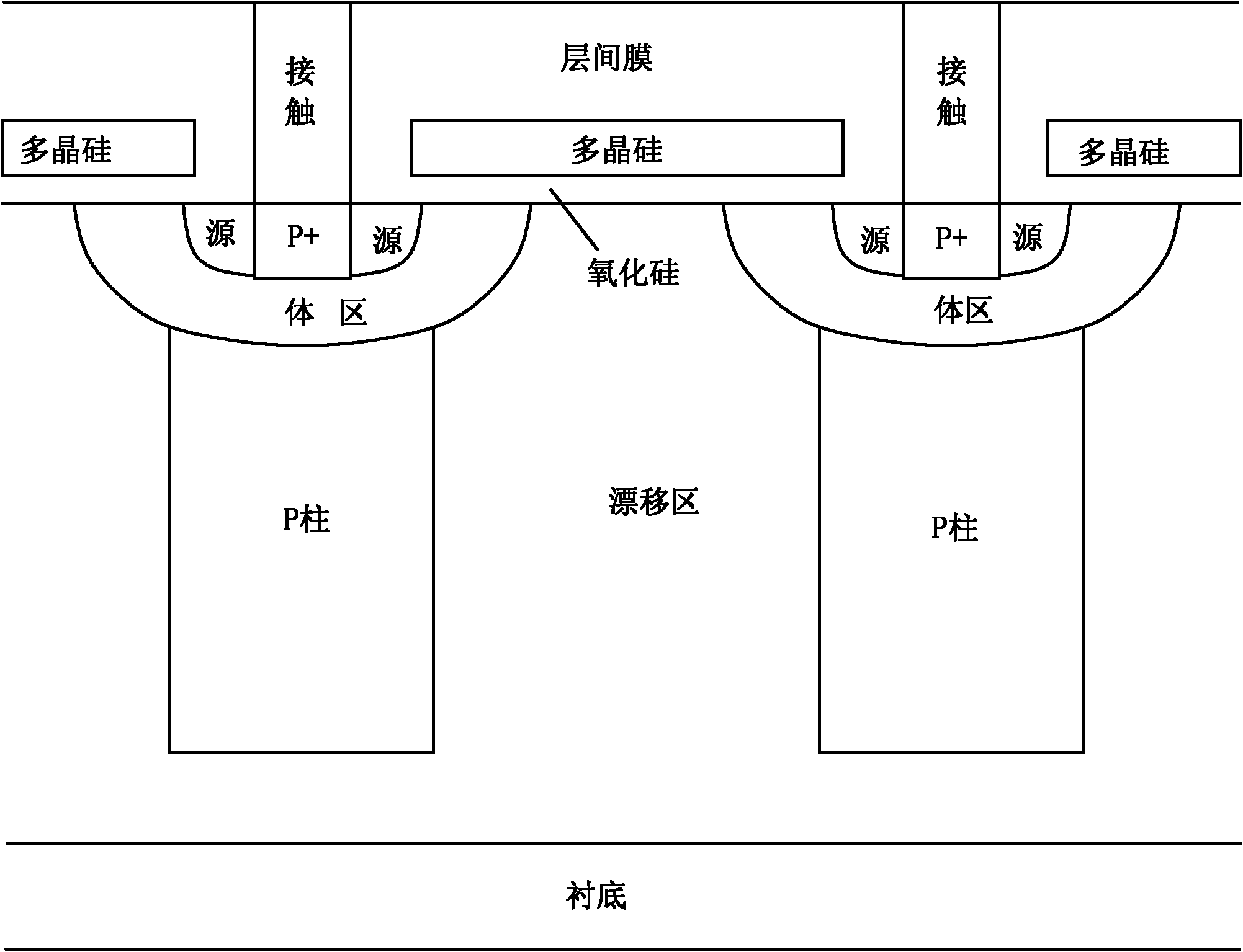
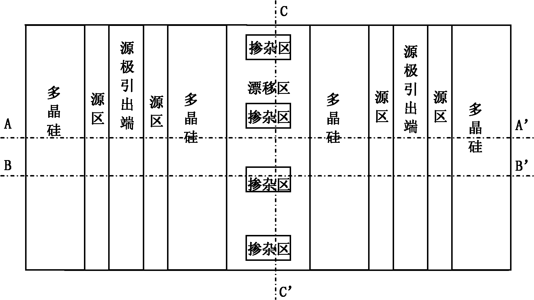
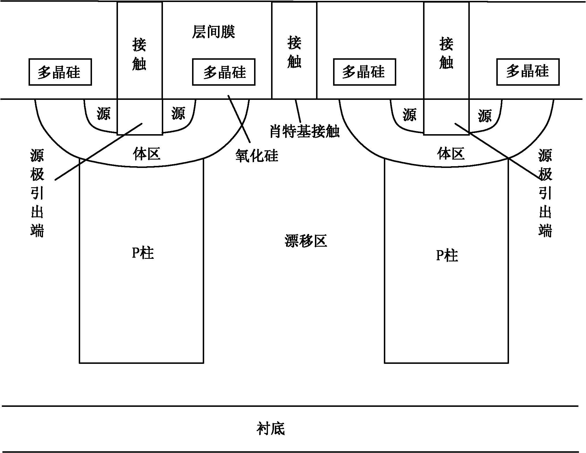
[0018] The structure of integrating the Schottky diode in the super junction MOSFET of the present invention is to connect the Schottky diode in parallel in the super junction MOSFET. The anode of the Schottky diode is arranged on the drift region between the two body regions at the source end of the super junction MOSFET cell region, a Schottky contact is formed by the anode and the drift region, and the anode is connected to the source end of the super junction MOSFET; The cathode of the Schottky diode shares the drain electrode of the superjunction MOSFET located on the backside of the substrate. On the drift region of the anode of the Schottky diode, there are also multiple doped regions. The conductivity type of the doped region is opposite to that of the drift region, and the impurity concentration is greater than that of the drift region. The doped region is also compatible with the source of the super junction MOSFET. end connected. The doped region adjacent to the Sc...


PUM


Abstract

The invention discloses a method for integrating a Schottky diode in a super-junction MOSFET (metal-oxide-semiconductor field effect transistor). In order to connect and combine the Schottky diode consisting of a Schottky contact and a substrate in the super-junction MOSFET in parallel, the anode of the Schottky diode is positioned on a drift area between two body areas at a source end of the super-junction MOSFET element cell area, and is connected with the source end of the super-junction MOSFET; a plurality of doping areas are arranged on the drift area of the anode, the electric conduction types of the doping areas are opposite to the electric conduction type of the drift area, the concentration of impurity is larger than that of impurity in the drift area, and the doping areas are connected with the source end of the super-junction MOSFET; and the cathodes of the Schottky diode share the drain electrode of the super-junction MOSFET. According to the method, the reverse electric leakage amount of the Schottky diode can be reduced.

Description

technical field [0001] The invention relates to a preparation method of a super junction MOSFET. Background technique [0002] Power Metal Oxide Semiconductor Field Effect Transistor (referred to as power MOS) inherently has a parasitic diode connected in parallel with it. The anode of the parasitic diode is connected to the body region and source of the MOS, and the cathode is connected to the drain of the MOS. Therefore, the power MOS is often used for freewheeling or clamping voltage. [0003] During freewheeling or clamping voltage, the parasitic diode is forward-conducting, and the MOS is also conducting. The voltage of the source (anode of the parasitic diode) of the MOS is slightly higher than the voltage of the drain (cathode of the parasitic diode), and the current flows from the source to the drain; The drain (cathode of the parasitic diode) voltage of the MOS is higher than the voltage of the source (anode of the parasitic diode) at the time of cut-off, and the d...

Claims


Application Information

Patent Timeline
IPC IPC(8): H01L21/336H01L29/78H01L29/06H01L29/872
CPCH01L29/7806H01L29/0634H01L29/0696
Inventor 金勤海王永成陈正嵘
Owner SHANGHAI HUAHONG GRACE SEMICON MFG CORP
Why Eureka
Try Eureka