Method for producing nano fluorescent powder-free gallium nitride white light-emitting diode

A light-emitting diode, no phosphor technology, applied in electrical components, circuits, semiconductor devices, etc., can solve problems such as reducing the Droop effect and increasing the luminous efficiency

Active Publication Date: 2012-07-25
INST OF SEMICONDUCTORS - CHINESE ACAD OF SCI
View PDF7 Cites 14 Cited by
  • Summary
  • Abstract
  • Description
  • Claims
  • Application Information

AI Technical Summary

Problems solved by technology

At the same time, this technology can also solve the stress problem caused by the lattice mismatch between the existing GaN material and InGaN material. Since this method uses a nano-template substrate, it can release the stress well, thereby reducing the Droop effect and increasing LED performance. Luminous efficiency
Since this method can solve problems that cannot be solved by conventional GaN LEDs, it will play an important role in the next generation of LEDs

Method used


Image

  • Method for producing nano fluorescent powder-free gallium nitride white light-emitting diode
  • Method for producing nano fluorescent powder-free gallium nitride white light-emitting diode
  • Method for producing nano fluorescent powder-free gallium nitride white light-emitting diode

Examples


Embodiment

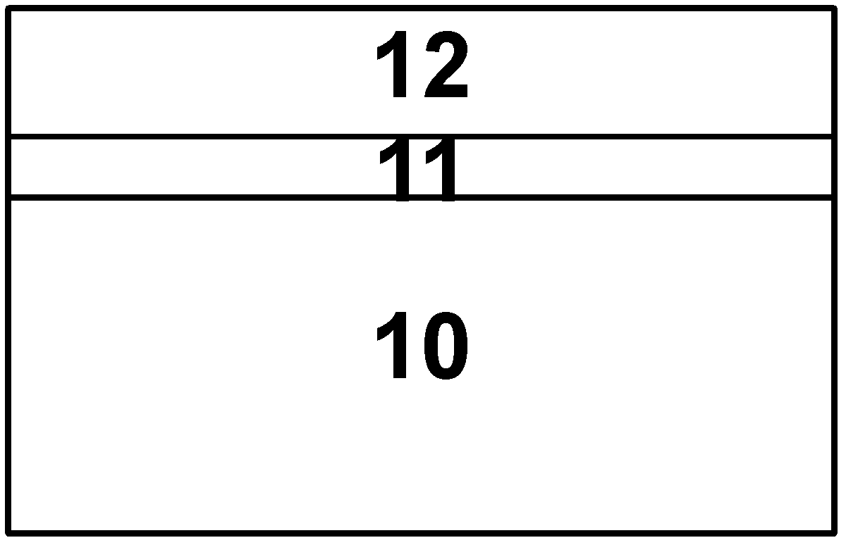
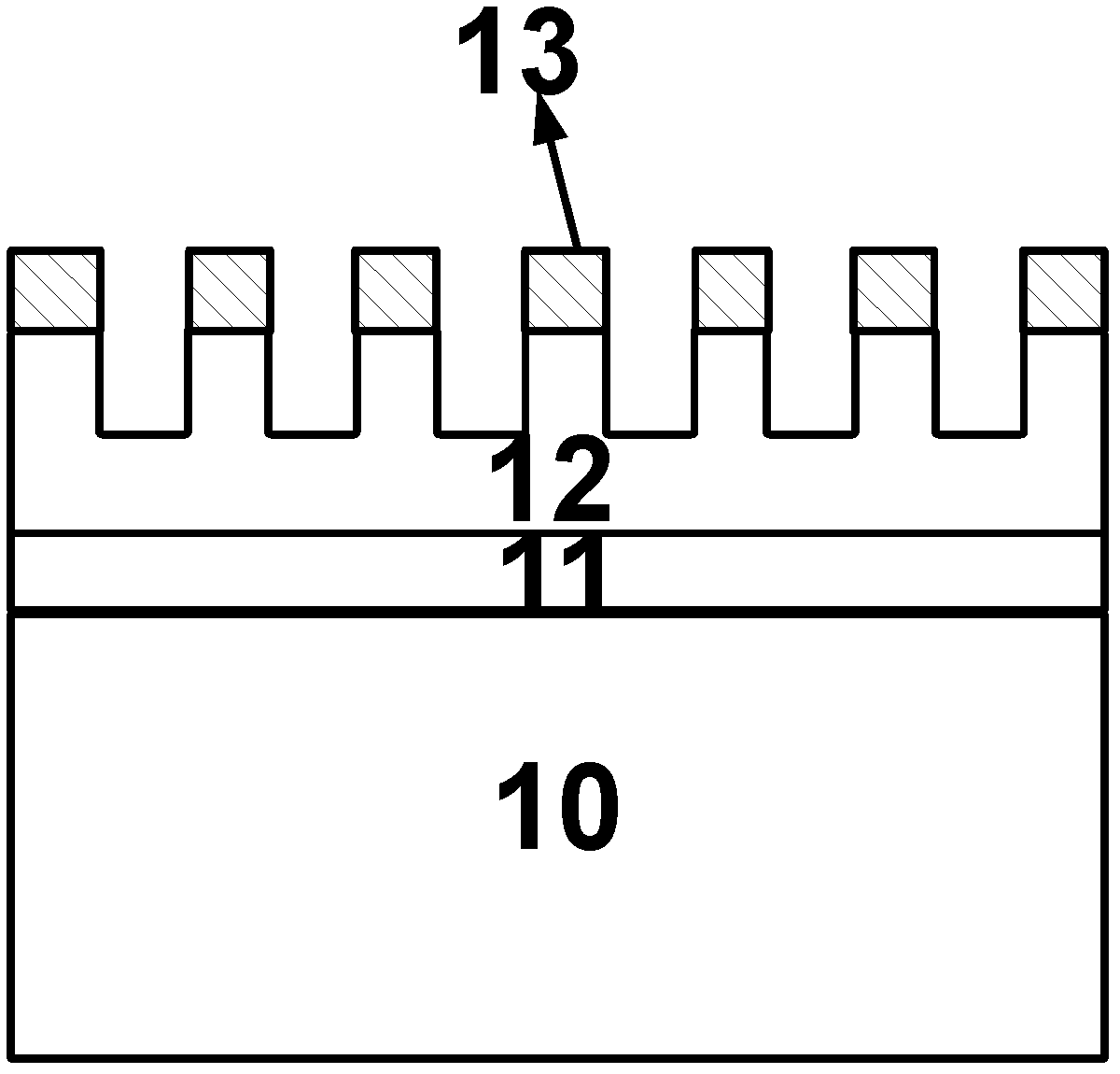
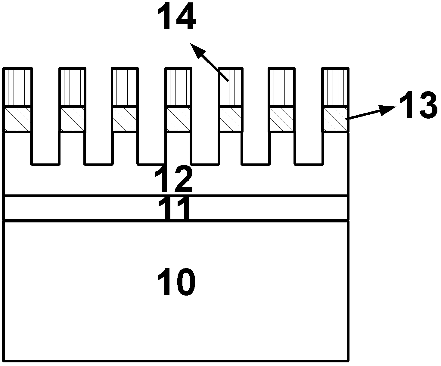
[0027] see figure 1 As shown in -6, the present invention provides a method for making a nano-phosphor gallium nitride white light-emitting diode, comprising the following steps:

[0028] Step 1: Take a substrate 10, which is sapphire and has a thickness of 400um.

[0029] Step 2: GaN buffer layer 11 and n-GaN layer 12 are epitaxially grown on the substrate 10, the thicknesses of GaN buffer layer 11 and n-GaN layer 12 are 2um and 3um respectively.

[0030] Step 3: Fabricate a GaN nanowire template on the n-GaN layer 12 by nanotechnology. The size of the nano-pattern template is 100nm, and the depth is 500nm.

[0031] Step 4: growing a GaN transition layer 13 on the GaN nanowire template. The thickness of the GaN transition layer 13 is 20 nm.

[0032] Step 5: growing the InGaN quantum disk 14 on the GaN transition layer 14 . The InGaN quantum disk 14 is 5 groups of InGaN / GaN, and the variation of the In composition is 0.15-0.3.

[0033] Step 6: growing a p-GaN layer 15 o...


PUM

PropertyMeasurementUnit
sizeaaaaaaaaaa

Abstract

A method for producing a nano fluorescent powder-free gallium nitride white light-emitting diode comprises the following steps that: step 1, a substrate is taken; step 2, a GaN buffer layer 1 and an n-GaN layer are epitaxially grown on the substrate; step 3, a GaN nano line template is produced on the n-GaN layer through a nano technology; step 4, a GaN transition layer is grown on the GaN nano line template; step 5, an InGaN quantum disc is grown on the GaN transition layer; step 6, a p-GaN layer is grown on the InGaN quantum disc to form a chip; step 7, the part of one side of the chip is etched, the etching depth reaches the inner side of the n-GaN layer to form a table board; step 8, a lower electrode is produced on the table board of the n-GaN layer; and step 9, an upper electrode is produced on the n-GaN layer to complete the production of the light-emitting diode. Because the method adopts the substrate of the nano template, the strain can be better released, accordingly, the Droop effect is reduced, and the luminous efficiency of the LED (light-emitting diode) is increased.

Description

technical field [0001] The invention belongs to the technical field of semiconductor lighting, in particular to a method for manufacturing a nanometer non-phosphor gallium nitride white light emitting diode. Background technique [0002] Gallium nitride is a third-generation semiconductor material with a bandgap of 3.4ev. Because of its stable properties and a direct bandgap luminescent material with a wavelength of blue-violet light, it is ideal for manufacturing blue-violet light-emitting diodes (LEDs) with high mobility. For high-rate transistor materials, National Semiconductor Lighting lists gallium nitride materials as the center. But at present, light-emitting diodes are facing a big problem. The method of exciting yellow phosphor powder with blue light to obtain white light-emitting diodes is currently adopted by the industry. Due to the luminous efficiency of the phosphor itself, the patent issue of the phosphor, and the scope and reliability of the color rendering...

Claims


Application Information

Patent Timeline
Patent Type & Authority Applications(China)
IPC IPC(8): H01L33/00
Inventor 孙波赵丽霞伊晓燕刘志强魏学成王国宏
Owner INST OF SEMICONDUCTORS - CHINESE ACAD OF SCI
Why Eureka
Try Eureka