Unlock instant, AI-driven research and patent intelligence for your innovation.

Magnetic random access memory and manufacturing method thereof

A technology of random access memory and manufacturing method, which is applied in static memory, digital memory information, manufacturing/processing of electromagnetic devices, etc., and can solve the problems of reduced current value and inability to ensure current, etc.

Active Publication Date: 2012-07-25
KIOXIA CORP +1
View PDF4 Cites 1 Cited by
  • Summary
  • Abstract
  • Description
  • Claims
  • Application Information

AI Technical Summary

Problems solved by technology

However, in this case, there are parasitic impedances such as the contact resistance (resistance) between the drain and the contact plug, the resistance of the contact plug itself, and the contact resistance between the contact plug and the electrode of the magnetoresistance effect element. When the magnetoresistance effect element flows, the current value decreases
Therefore, there arises a problem that the current necessary for reversing the magnetization of the magnetoresistance effect element cannot be ensured.

Method used


Image

  • Magnetic random access memory and manufacturing method thereof
  • Magnetic random access memory and manufacturing method thereof
  • Magnetic random access memory and manufacturing method thereof

Examples


no. 1 approach

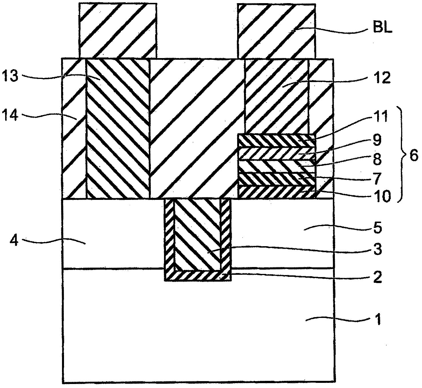
[0016] Hereinafter, the magnetic random access memory according to the first embodiment will be described. figure 1 as well as figure 2 It is a cross-sectional view showing a memory cell in the magnetic random access memory according to the first embodiment.

[0017] Such as figure 1 As shown, a selection transistor is embedded in the surface portion of a semiconductor substrate, for example, a silicon substrate 1 . The selection transistor includes a gate insulating film 2 , a gate electrode 3 , a source diffusion layer 4 and a drain diffusion layer 5 .

[0018] For the silicon substrate 1 , for example, a p-type silicon substrate is used. A gate electrode 3 is embedded in the surface portion of the silicon substrate 1 . For the gate electrode 3, polysilicon, W, or the like is used, for example. Gate insulating film 2 is embedded in silicon substrate 1 so as to cover gate electrode 3 . For the gate insulating film 2, for example, a silicon oxide film is used. The heig...

no. 2 approach

[0053] Regarding the magnetic random access memory according to the second embodiment of the present invention, using Figure 4 Be explained. Regarding the configuration of the second embodiment, for the figure 1 The same components of the magnetic random access memory of the first embodiment are denoted by the same symbols, and detailed description thereof will be omitted.

[0054] The magnetic random access memory according to the second embodiment is the same as that of the first embodiment in that buried transistors are used. On the other hand, the second embodiment is different from the first embodiment in that the embedded transistor is not buried in the silicon substrate 1 but is buried in a semiconductor layer such as the silicon film 18 . Specifically, the difference is that instead of embedding the gate insulating film 2 and the gate electrode 3 in the silicon substrate 1, the gate insulating film 2 and the gate electrode 3 are provided on the silicon substrate 1 s...

no. 3 approach

[0067] Regarding the magnetic random access memory according to the third embodiment of the present invention, using Figure 6 Be explained. Regarding the configuration of the third embodiment, for the figure 1 The same components of the magnetic random access memory of the first embodiment shown are denoted by the same symbols, and detailed description thereof will be omitted.

[0068] The third embodiment differs from the first embodiment in that the gate insulating film 2 and the gate electrode 3 are not embedded in the silicon substrate 1 but are provided on the silicon substrate 1 .

[0069] For the manufacturing method of the magnetic random access memory in the third embodiment of the present invention, using Figure 7A to Figure 7F Be explained.

[0070] Such as Figure 7A As shown, a gate insulating film 2 and a gate electrode 3 are deposited on a silicon substrate 1, and the gate insulating film 2 and the gate electrode 3 are formed by photolithography and RIE. ...


PUM


Abstract

The invention provides a magnetic random access memory and the manufacturing method thereof. According to one embodiment, there is disclosed a magnetic random access memory comprising: a semiconductor substrate; a selective transistor formed at the surface region of the semiconductor substrate and having a gate electrode, a gate insulating film, a source and a drain; and a magnetoresistive element formed on the drain including a magnetic storage layer in which a magnetization direction is variable, a magnetic reference layer in which a magnetization direction is fixed, and a nonmagnetic layer sandwiched between the magnetic storage layer and the magnetic reference layer.

Description

technical field [0001] The present invention relates to a magnetic random access memory and a manufacturing method thereof. Background technique [0002] In recent years, a magnetic random access memory (MRAM: Magnetic Random Access Memory) utilizing a tunneling magnetoresistance effect (TMR: Tunneling Magneto Resistive) has been developed. In this magnetic random access memory, a magnetoresistance effect element including a magnetic tunnel junction (MTJ: Magnetic Tunnel Junction) is used, and has a large magnetoresistance change rate. [0003] In the spin injection writing method currently under study, the direction of magnetization in the magnetoresistance effect element is reversed by injecting a current into the magnetoresistance effect element. At this time, generally, the current flowing to the magnetoresistance effect element flows from the drain of the MISFET (Metal-Insulator-Semiconductor Field-Effect Transistor) through the contact plug. However, in this case, th...

Claims


Application Information

Patent Timeline
Patent Type & Authority Applications(China)
IPC IPC(8): H01L43/08H01L43/12H01L27/22G11C11/15
CPCG11C11/16H01L27/228G11C11/161G11C11/1659H10B61/22H10N50/10H10N50/01
Inventor 野町映子
Owner KIOXIA CORP