Charge pump and charge pump system

A charge pump and circuit technology, applied in the direction of conversion equipment without intermediate conversion to AC, can solve the problems affecting the transmission efficiency of the charge pump, and achieve the effect of eliminating the lining effect, improving the transmission efficiency, and improving the reliability

Active Publication Date: 2012-08-01
SHANGHAI HUAHONG GRACE SEMICON MFG CORP
View PDF5 Cites 8 Cited by
  • Summary
  • Abstract
  • Description
  • Claims
  • Application Information

AI Technical Summary

Problems solved by technology

The MOS tube with this structure has a lining bias effect. As the voltage value of the output voltage of the upper-stage charge pump increases, this lining bias effect will become more obvious, thereby affecting the transmission efficiency of the charge pump.

Method used


Image

  • Charge pump and charge pump system
  • Charge pump and charge pump system
  • Charge pump and charge pump system

Examples


Embodiment 1

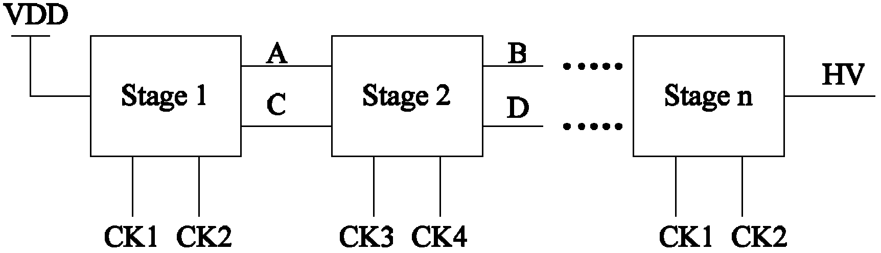
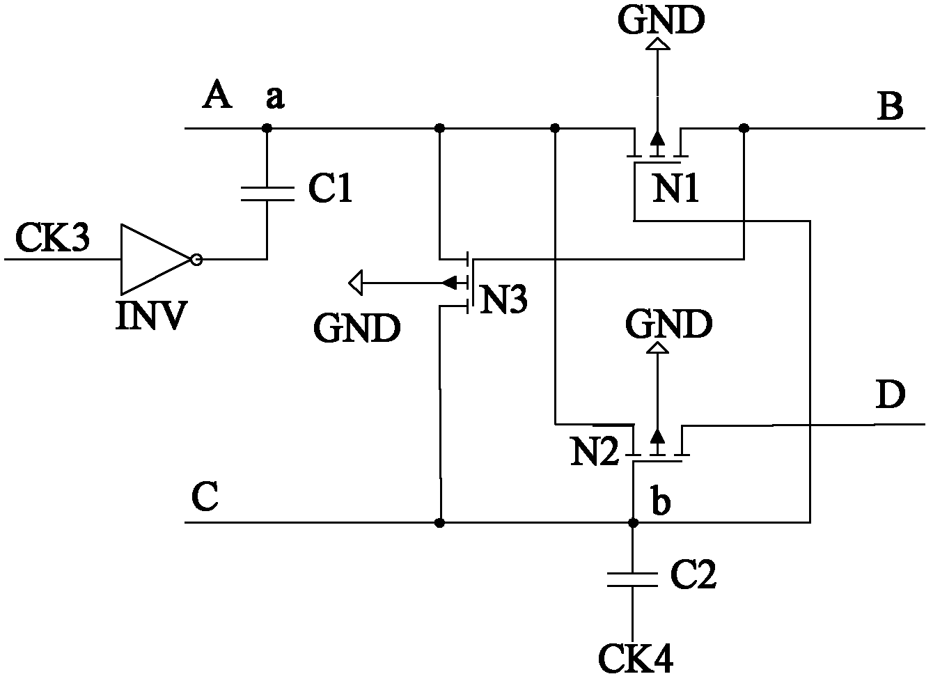
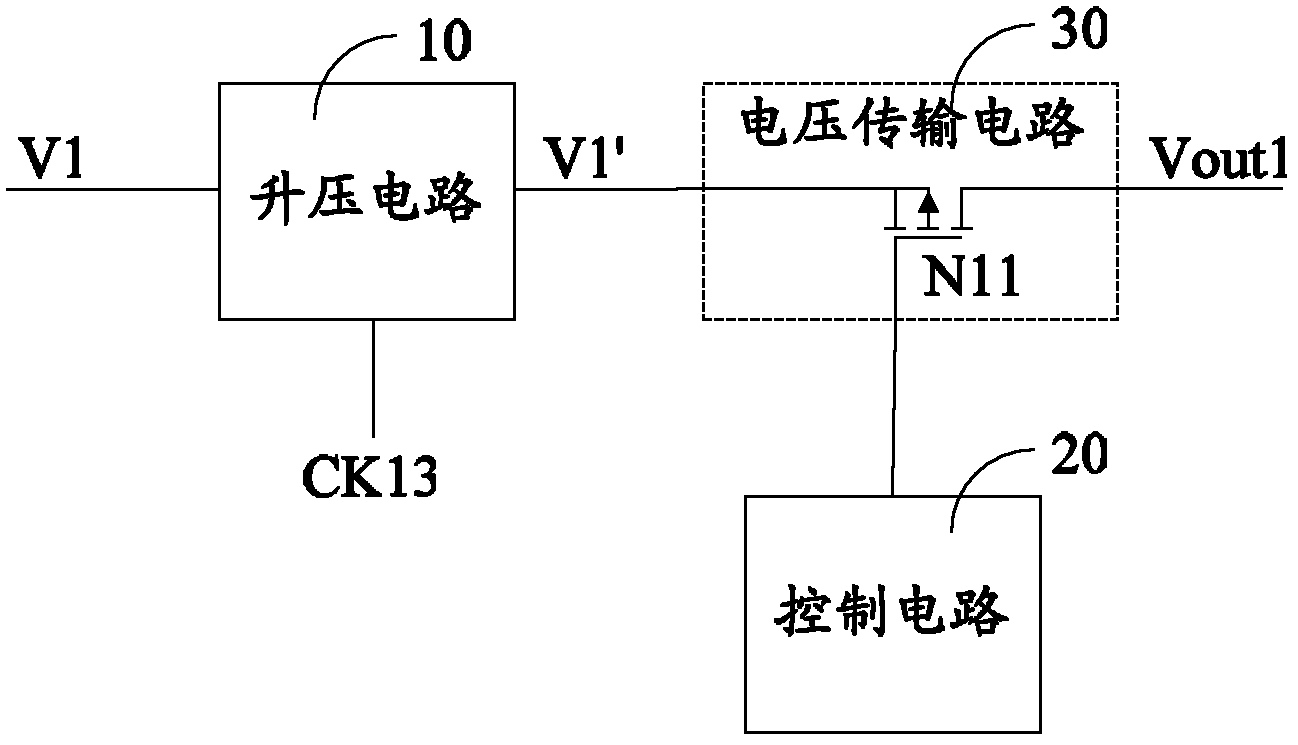
[0048] Figure 5 A schematic diagram of Embodiment 1 of the charge pump of the present invention is shown. Such as Figure 5 As shown, the charge pump includes a boost circuit 10 , a control circuit 20 and a voltage transmission circuit 30 .

[0049] The voltage transmission circuit 30 includes a first NMOS transistor N11. The source of the first NMOS transistor N11 is commonly connected to the node e with the output terminal of the booster circuit 10, the gate is commonly connected to the node f with the control circuit 20, and the drain is used as the first output terminal of the charge pump , for the output voltage Vout1.

[0050] The boost circuit 10 includes: a first capacitor C11 and an inverter INV1. One end of the first capacitor C11 is connected to the source of the first NMOS transistor N11, that is, the node e, and the other end is connected to the output end of the inverter INV1, and the input end of the inverter INV1 receives the first Control signal CK13.

...

Embodiment 2

[0072] Figure 6 A schematic diagram of Embodiment 2 of the charge pump of the present invention is shown. refer to Figure 6, compared with Embodiment 1, the charge pump of this embodiment further includes a third NMOS transistor N13.

[0073] The source of the third NMOS transistor N13 is connected to the source of the first NMOS transistor N11, the gate is connected to the drain of the first NMOS transistor N11, and the drain is connected to the gate of the first NMOS transistor N11 and receives the first NMOS transistor N11. Two input voltage V2.

[0074] Moreover, in this embodiment, the third NMOS transistor N13 includes a P-type substrate, an N-type well region is included in the P-type substrate, a P-type well region is included in the N-type well region, and a P-type well region is included in the N-type well region. The P-type well region includes an N-type doped source region and a drain region; the substrate of the third NMOS transistor is connected to the sourc...


PUM


Abstract

Disclosed are a charge pump and a charge pump system. The charge pump comprises a boosting circuit, a control circuit and a voltage transmission circuit. The boosting circuit is used for boosting first input voltage according to first control signals, the voltage transmission circuit comprises a first NMOS (N-metal oxide semiconductor) tube, a source electrode of the first NMOS tube is connected with the boosting circuit, a grid of the NMOS tube is connected with the control circuit, and a drain of the NMOS tube serves as a first output end of the charge pump. The control circuit is used for controlling on and off of the first NMOS tube, and the first NMOS tube outputs the first input voltage after being boosted when being on and comprises a P-shaped substrate. The P-shaped substrate comprises an N-shaped trap area, the N-shaped trap area comprises a P-shaped trap area, the P-shaped trap area comprise an N-shaped doped source electrode area and a drain area, and the P-shaped substrate and the N-shaped trap area of the first NMOS tube are respectively connected with the source electrode area. By the charge pump, an MOS (metal oxide semiconductor) is protected from breakdown, reliability of the circuit is improved, lining deviation effect of the MOS tube is eliminated, and transmission efficiency of the charge pump is improved.

Description

technical field [0001] The invention relates to the technical field of integrated circuits, in particular to a charge pump and a charge pump system. Background technique [0002] In the information age, various types of memory are used more and more widely. Based on the requirements of low power consumption and low cost, the power supply voltage of the memory is usually relatively low, such as 2.5V, 1.8V, etc. The program voltage and erase voltage, such as 8V or 11V and so on. Therefore, charge pump circuits are widely used in memories to obtain higher programming voltages or erasing voltages through lower power supply voltages. [0003] figure 1 A schematic structural diagram of a charge pump system in the prior art is shown. Such as figure 1 As shown, the power supply voltage VDD passes through a multi-stage charge pump, such as figure 1 The first-order charge pump Stage 1, the second-order charge pump Stage 2, and the N-stage charge pump Stage n shown in the figure ...

Claims


Application Information

Patent Timeline
Patent Type & Authority Applications(China)
IPC IPC(8): H02M3/07
Inventor 杨光军胡剑吴常谦
Owner SHANGHAI HUAHONG GRACE SEMICON MFG CORP
Why Eureka
Try Eureka