Array substrate and manufacturing method thereof, liquid crystal panel, and display device

An array substrate and substrate technology, applied in the field of liquid crystal panels and display devices, array substrates and manufacturing methods thereof, can solve problems such as easy peeling, diffusion, and affecting the conduction performance of TFT structures, and achieve the effect of increasing adhesion

Inactive Publication Date: 2012-08-08
BOE TECH GRP CO LTD
View PDF4 Cites 39 Cited by
  • Summary
  • Abstract
  • Description
  • Claims
  • Application Information

AI Technical Summary

Problems solved by technology

[0007] In the process of realizing the TFT structure of the above-mentioned liquid crystal display, the inventor found that there are at least the following problems in the prior art: 1) the adhesion between Cu and the substrate

Method used


Image

  • Array substrate and manufacturing method thereof, liquid crystal panel, and display device
  • Array substrate and manufacturing method thereof, liquid crystal panel, and display device
  • Array substrate and manufacturing method thereof, liquid crystal panel, and display device

Examples


Embodiment 1

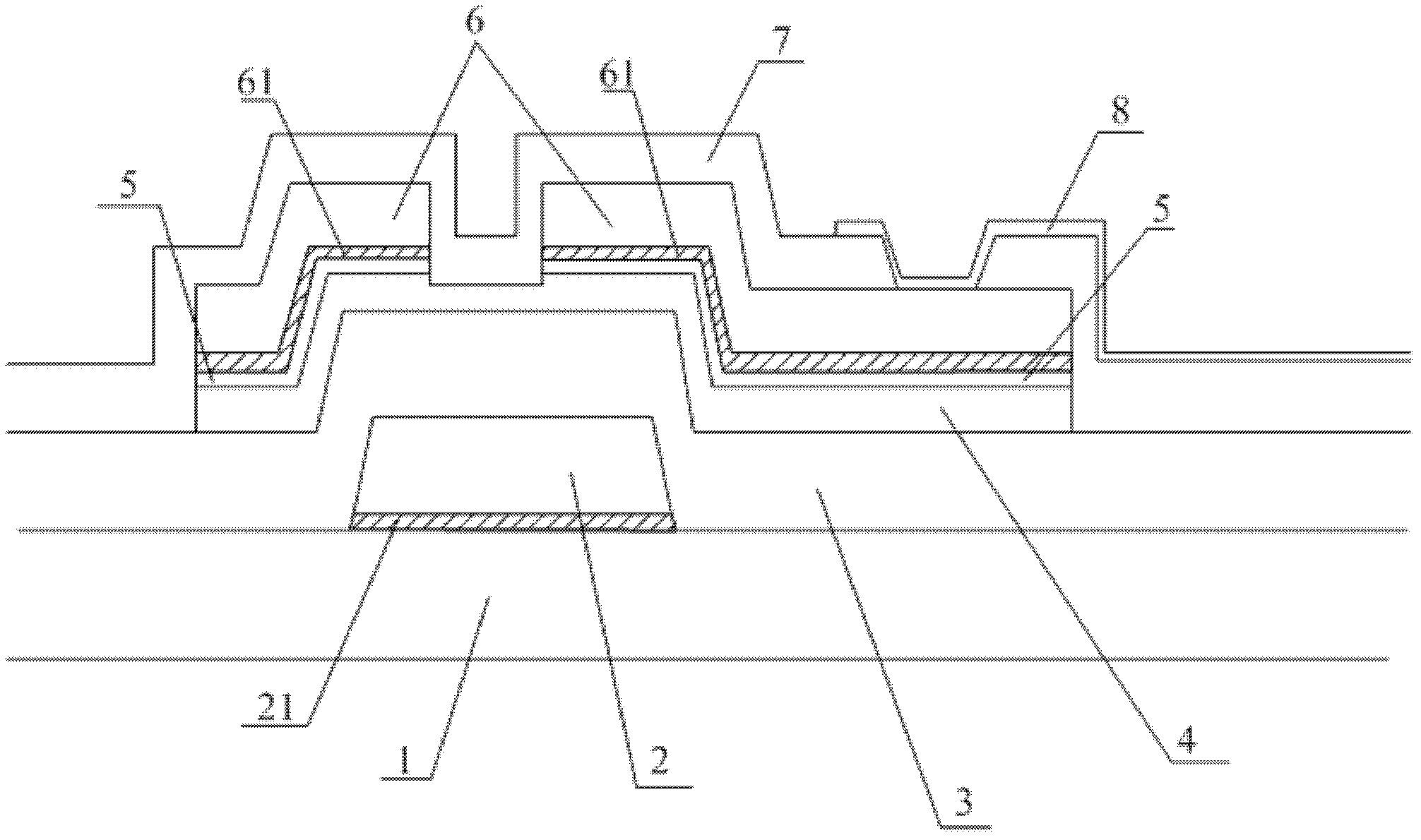
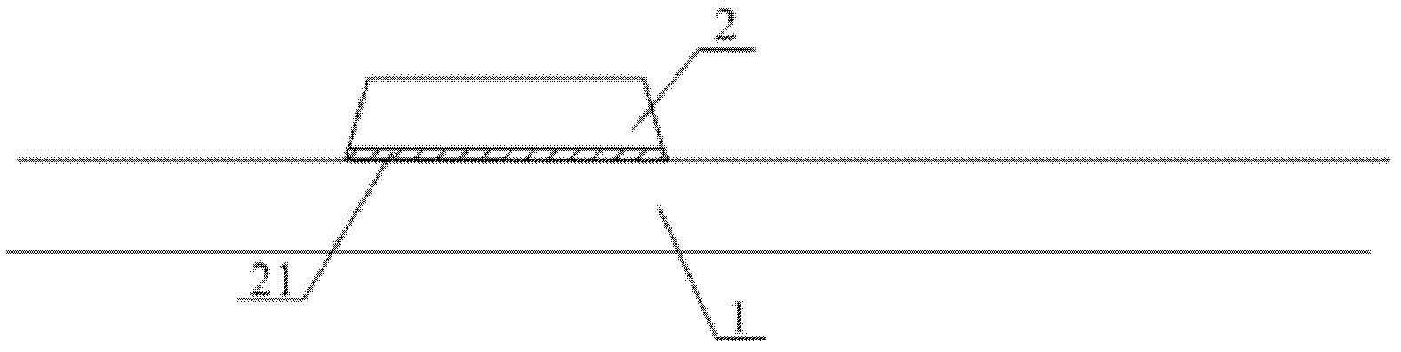
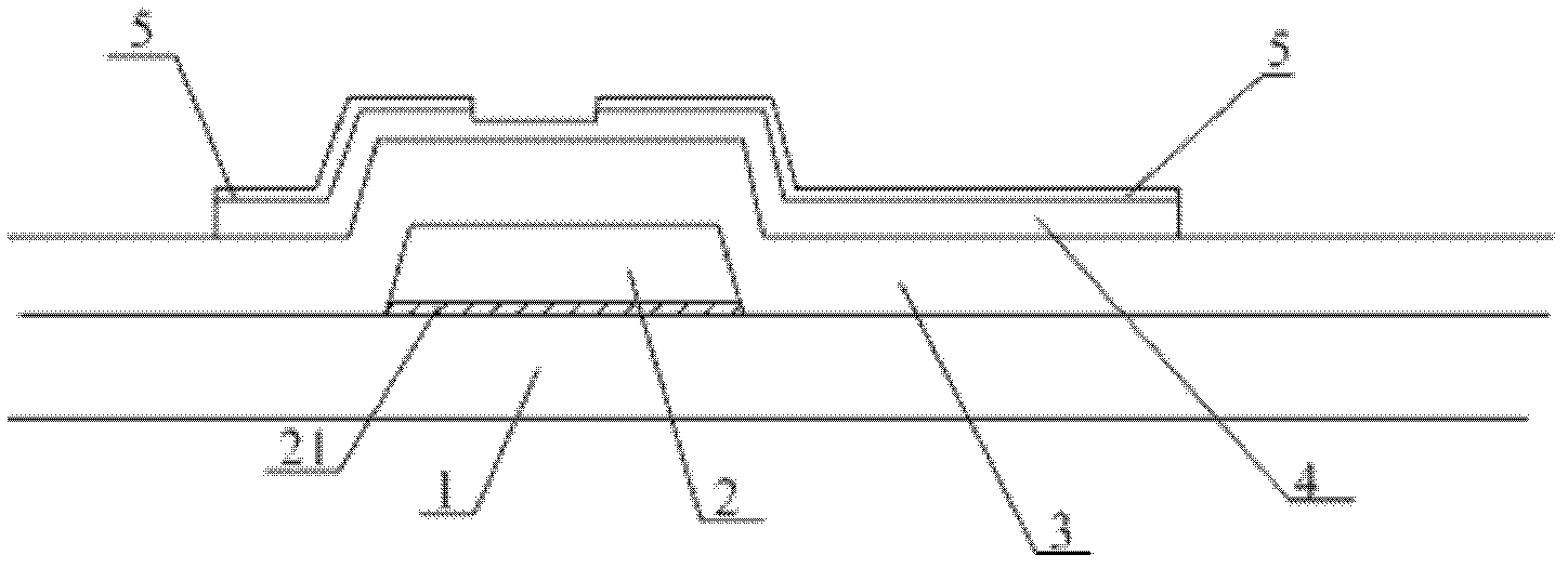
[0046] like figure 1 As shown, an array substrate provided by an embodiment of the present invention includes a substrate 1 and a gate metal layer 2, a gate insulating layer 3, a semiconductor layer 4, an ohmic contact layer 5, and a source / drain metal layer 6 formed on the substrate 1. , and the passivation layer 7 and the pixel electrode 8; wherein, a first isolation buffer layer 21 is formed between the gate metal layer 2 and the substrate 1, and a second isolation buffer layer 21 is formed between the ohmic contact layer 5 and the source / drain metal layer 6 Isolation buffer layer 61;

[0047] Wherein, the substrate 1 may be, but not limited to, a glass substrate or a quartz substrate;

[0048] The gate metal layer 2 and the source / drain metal layer 6 take metal Cu as an example in this embodiment;

[0049] The gate insulating layer 3 is made of Si x N y (silicon nitride) or Si x o y (silicon oxide) and other silicon series materials;

[0050] The semiconductor layer 4...

Embodiment 2

[0076] On the basis of the array substrate provided in Embodiment 1, this embodiment further improves it to obtain another array substrate structure. specifically,

[0077] like image 3 As shown, another array substrate provided in this embodiment includes a substrate 1 and a gate metal layer 2, a gate insulating layer 3, a semiconductor layer 4, an ohmic contact layer 5 and a source / drain metal layer 6 formed on the substrate 1. , and the passivation layer 7 and the pixel electrode 8; wherein, a first isolation buffer layer 21 is formed between the gate metal layer 2 and the substrate 1, and a second isolation buffer layer 21 is formed between the ohmic contact layer 5 and the source / drain metal layer 6 Isolation buffer layer 61;

[0078] In addition, a third isolation buffer layer 22 is formed between the gate metal layer 2 and the gate insulating layer 3 .

[0079] Wherein, the gate metal layer 2 and the source / drain metal layer 6 are metal Cu in this embodiment;

[00...

Embodiment 3

[0087] On the basis of the array substrate provided in Embodiment 1, this embodiment further improves it to obtain another array substrate structure. specifically,

[0088] like Figure 4 As shown, another array substrate provided in this embodiment includes a substrate 1 and a gate metal layer 2, a gate insulating layer 3, a semiconductor layer 4, an ohmic contact layer 5 and a source / drain metal layer 6 formed on the substrate 1. , and the passivation layer 7 and the pixel electrode 8; wherein, a first isolation buffer layer 21 is formed between the gate metal layer 2 and the substrate 1, and a second isolation buffer layer 21 is formed between the ohmic contact layer 5 and the source / drain metal layer 6 Isolation buffer layer 61;

[0089] In addition, a fourth isolation buffer layer 62 is formed between the source / drain metal layer 6 and the passivation layer 7 .

[0090] Wherein, the gate metal layer 2 and the source / drain metal layer 6 are metal Cu in this embodiment; ...


PUM


Abstract

The embodiments of the invention, which relates to the liquid crystal display technology field, disclose an array substrate and a manufacturing method thereof, a liquid crystal panel, and a display device, thereby effectively preventing metal ions of a metal electrode layer from in a thin film transistor (TFT) structure being diffused to a film layer of silicon series and strengthening an adhesive force between the metal electrode layer and a substrate. The provided array substrate comprises a substrate body, a gate metal layer, an active layer and a source/drain metal layer, wherein the gate metal layer, the active layer and the source/drain metal layer are formed on the substrate. An isolation buffer layer is formed at at least one side of the gate metal layer and/or an isolation buffer layer is formed at at least one side of the source/drain metal layer; and moreover, the isolation buffer layers are formed by molybdenum oxide. According to the embodiments of the invention, the provided schemes are suitable for various display devices employing TFT substrates and an X-ray detector device.

Description

technical field [0001] The invention relates to the technical field of liquid crystal display, in particular to an array substrate and a manufacturing method thereof, a liquid crystal panel and a display device. Background technique [0002] Existing display devices tend to be more and more diversified, and common ones include liquid crystal displays, e-book readers, OLED (Organic Light-Emitting Diode, Organic Light-Emitting Diode) displays, and the like. [0003] Taking liquid crystal display as an example, the gate and source / drain in the TFT (Thin Film Transistor, Thin Film Field Effect Transistor) structure of the liquid crystal display are used as metal electrodes in the array substrate, which need to have low resistance, and are compatible with the substrate and other films. layer (such as amorphous silicon, doped amorphous silicon layer) has good adhesion, does not produce ion diffusion in the a-Si (amorphous silicon) layer, has low contact resistance with the pixel e...

Claims


Application Information

Patent Timeline
IPC IPC(8): H01L27/12H01L21/77G02F1/1362G02F1/1368
CPCG02F1/1362H01L21/77H01L29/4908H01L29/458H01L33/0041H01L27/12H01L27/124G02F1/1368H01L27/15G02F1/136286H01L21/2855
Inventor 郭炜李禹奉
Owner BOE TECH GRP CO LTD
Why Eureka
Try Eureka