
Semiconductor device

A semiconductor and device technology, applied in the field of semiconductor devices, can solve problems such as error rewriting

Inactive Publication Date: 2016-03-09
RENESAS ELECTRONICS CORP
View PDF9 Cites 2 Cited by
  • Summary
  • Abstract
  • Description
  • Claims
  • Application Information

AI Technical Summary

Problems solved by technology

[0007] However, if the information rewriting current is reduced, there is a possibility that, for example, when information recorded in another memory cell is read, the recording in the (unintended) memory cell adjacent to the other memory cell The information is erroneously rewritten by the current passing at this time

Method used


Image

  • Semiconductor device
  • Semiconductor device
  • Semiconductor device

Examples


no. 1 example

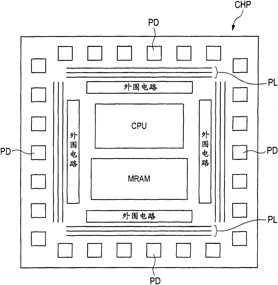
[0145] First, refer to figure 1 A description is given of the semiconductor device in the form of a chip in this embodiment.

[0146] Such as figure 1 As shown, the semiconductor chip CHP in this embodiment includes a CPU (Central Processing Unit), an MRAM, peripheral circuits, and a power supply line PL. Pads PD are placed in the peripheral region of the semiconductor chip CHP.

[0147] The CPU is a circuit also called a central processing unit, and it reads instructions from a storage device, interprets the instructions, and performs various calculations and controls based on the instructions. For this reason, high-speed processing of the CPU is required.

[0148] An MRAM is an element from which memory information can be read and written in a random fashion using magnetism. The MRAM has not only a function as a nonvolatile memory in which memory information is retained even after power is turned off, but also a high-speed random access function. The MRAM includes: a ...

no. 2 example

[0206] The second embodiment of the present invention differs from the first embodiment in the arrangement of the magnetoresistive element MRD and the configuration of the bit line BL. In the following, reference will be made to Figure 27 to Figure 47 A description is given of the configuration of this embodiment.

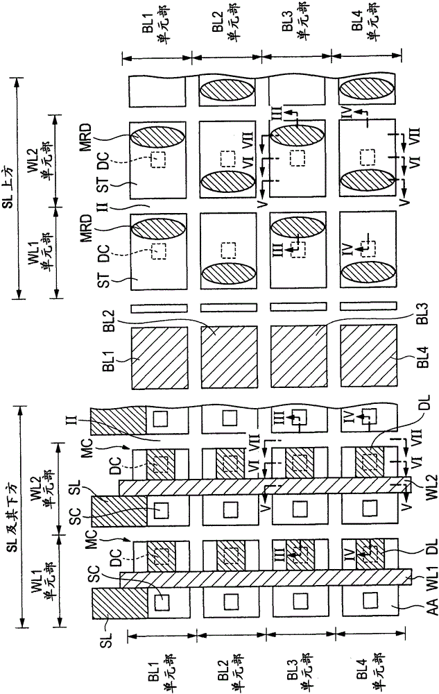
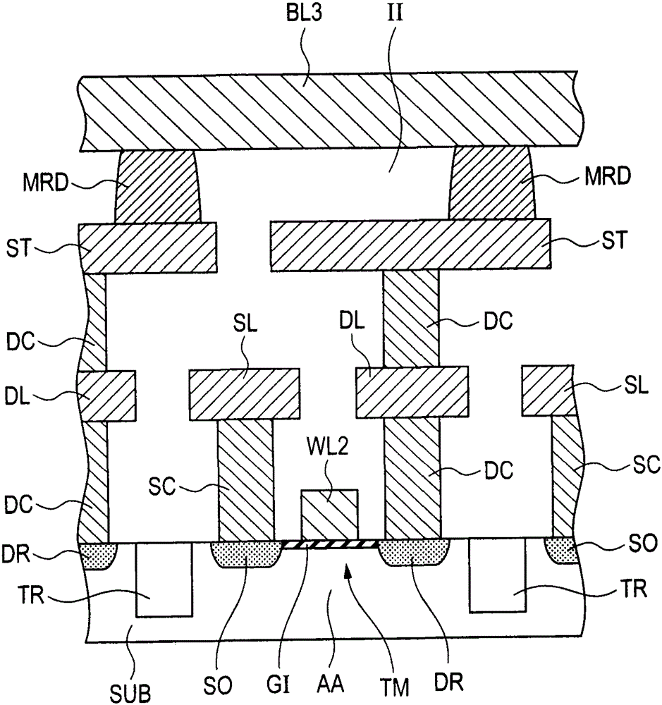
[0207] Such as Figure 27 As shown in , the memory cell region in the first example of this embodiment also has the same Figure 2 to Figure 7 The memory cell regions shown in the first embodiment are basically the same configuration. However, in Figure 27 In the example in , the magnetoresistive element MRD and the drain contact DC are arranged such that they overlap each other as seen in the plane.

[0208] A more specific description will be given. Among the magnetoresistive elements MRD arranged in a staggered configuration, the magnetoresistive elements MRD of the BL1 unit portion and the BL3 unit portion are placed on the right side of each strap wirin...

no. 3 example

[0236] The third embodiment of the present invention differs from the first embodiment in the arrangement of the source and drain contacts and the configuration of the source line SL. In the following, reference will be made to Figure 48 to Figure 77 A description is given of the configuration of this embodiment.

[0237] In the first example of this embodiment, as Figure 48 As shown in , the magnetoresistive elements MRD are arranged such that they are as in relation to the first embodiment figure 2 Arranged in a staggered configuration with respect to each strap wiring ST as in. In this embodiment, in addition to the above features, the source contacts SC and drain contacts DC are also arranged in a staggered configuration similarly to the magnetoresistive elements MRD.

[0238] A more specific description will be given. For example, in Figure 48The source contacts SC and drain contacts DC of two memory cells MC adjacent to each other in the vertical direction are a...


PUM


Abstract

A semiconductor device comprising: a spin moment written in-plane magnetized magnetoresistive element placed on a main surface of a semiconductor substrate, the magnetization state of which can be changed according to a current flow direction; and a first wiring, and the magnetoresistive element Electrically coupled and extending toward a direction along the major surface. The width-to-length ratio of the magnetoresistive element as seen in a plane is a value other than 1. In a memory cell region where a plurality of memory cells in which a magnetoresistive element and a switching element are electrically coupled to each other are arranged, measures are taken: a plurality of memory cells adjacent to each other in the length direction of each magnetoresistive element as seen in a plane The magnetoresistive elements are arranged such that they are not placed on the same straight line extending in the length direction.

Description

[0001] Cross References to Related Applications [0002] The entire disclosure of Japanese Patent Application No. 2011-22918 filed on February 4, 2011, including specification, drawings and abstract, is hereby incorporated by reference. technical field [0003] The present invention relates to semiconductor devices, and more particularly, to a semiconductor device having a magnetoresistive element. Background technique [0004] As semiconductor devices for storage, such as semiconductor integrated circuits, DRAM (Dynamic Random Access Memory) and SRAM (Static Random Access Memory) have conventionally been widely used. Meanwhile, MRAM (Magnetic Random Access Memory) is a device (magnetoresistive element) that stores information magnetically and has excellent features in high-speed operation, rewrite resistance, non-volatility, etc., compared to other memory technologies. [0005] In conjunction with recent miniaturization of semiconductor integrated circuits, inventions can...

Claims


Application Information

Patent Timeline
Patent Type & Authority Patents(China)
IPC IPC(8): H01L43/08H01L27/22
CPCG11C11/1655G11C11/1659G11C11/161G11C11/1675G11C11/14Y10S977/935H10B61/22H10N50/10G11C11/15H01L29/82H10B61/20H10B61/00H10N50/01H10N50/80B82Y10/00
Inventor 新田文彦
Owner RENESAS ELECTRONICS CORP
Learn More