Optical network-on-chip system based on wavelength allocation and communication method of system

An optical on-chip network and wavelength allocation technology, applied in the field of communication, can solve the problems of increasing the difficulty of manufacturing process and integration process, aggravating signal crosstalk, and increasing the number of wavelengths, so as to overcome the easy entry into the congestion state, reduce the number of wavelengths used, and overcome the wave guide. crossover effect

Inactive Publication Date: 2012-08-15
XIDIAN UNIV
View PDF3 Cites 29 Cited by
  • Summary
  • Abstract
  • Description
  • Claims
  • Application Information

AI Technical Summary

Problems solved by technology

At present, there are three main implementation schemes of optical network on chip based on wavelength division multiplexing: one is to assign a different wavelength to each node, and its disadvantage is that too many wavelengths are used, which limits the network scalability; the second is to assign a different wavelength to each node. It realizes wavelength reuse by adding waveguides and improves the utilization rate of wavelengths. The disadvantage is that the increase in the number of waveguides will increase the number of waveguide crossings a...

Method used


Image

  • Optical network-on-chip system based on wavelength allocation and communication method of system
  • Optical network-on-chip system based on wavelength allocation and communication method of system
  • Optical network-on-chip system based on wavelength allocation and communication method of system

Examples


Embodiment Construction

[0053] In order to more clearly introduce the optical network-on-chip system based on wavelength allocation proposed by the present invention, the following will describe in detail with reference to the accompanying drawings and specific examples.

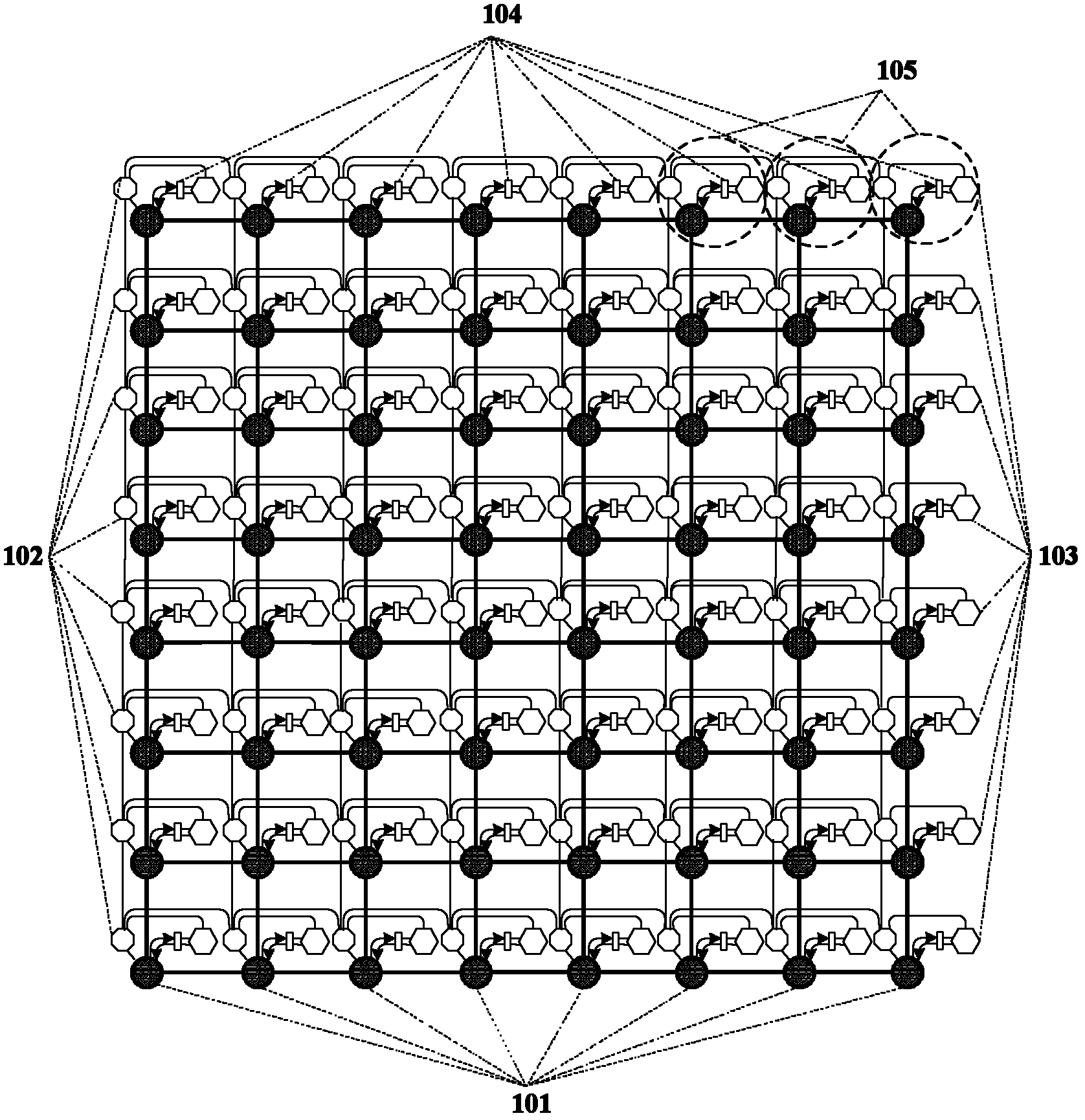
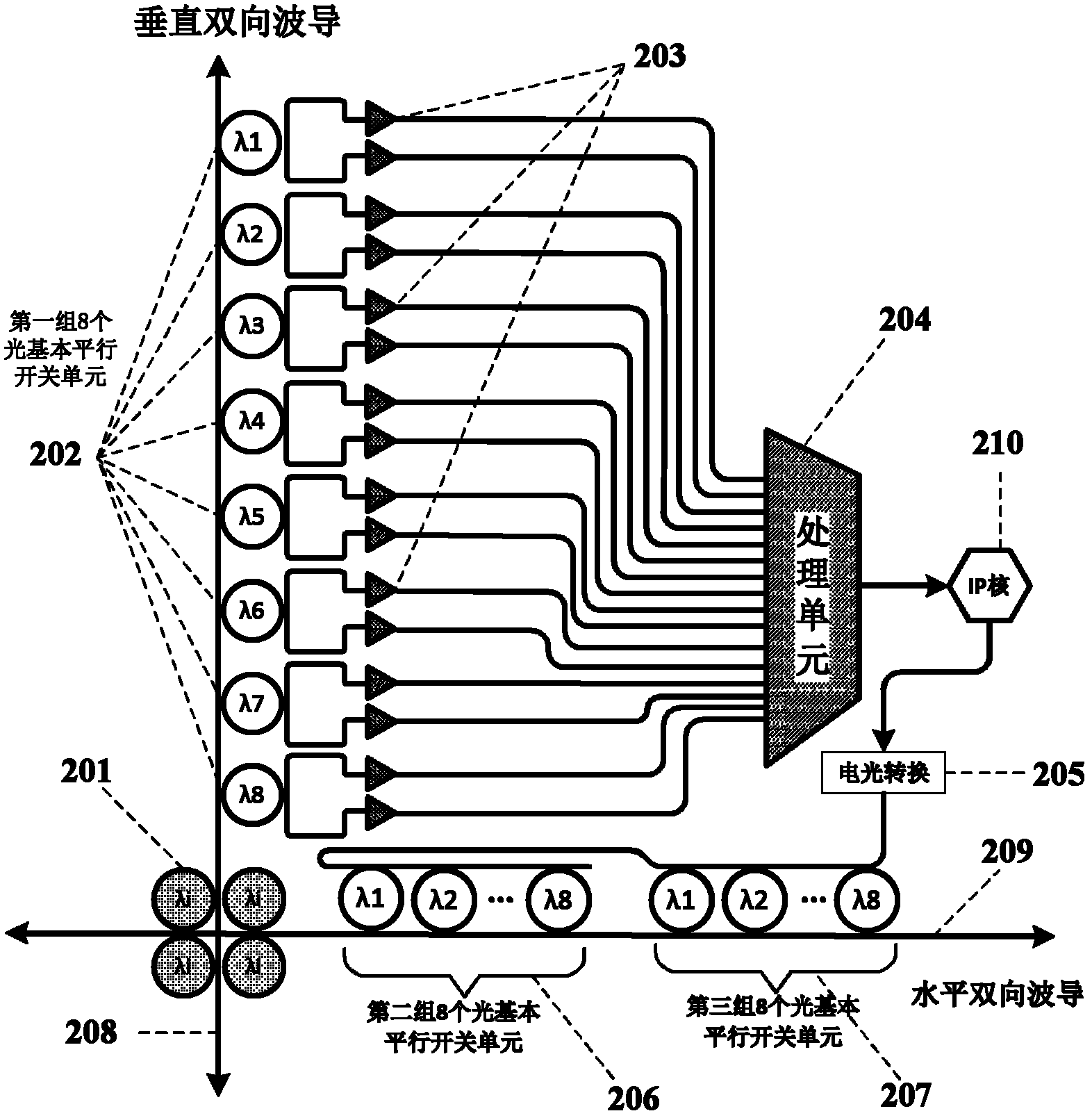
[0054] refer to figure 1 , the optical network-on-chip system based on wavelength allocation proposed by the present invention, including n 2 nodes 105, n is the dimension of n×n grid-like optical network on chip, 3≤n≤32, each node includes 1 IP core 103, 1 optical router 101, 1 electrical router 102, and 1 The electro-optical conversion unit 104, one photoelectric conversion unit 104 and one processing unit, n=8 in this example. All optical routers in the system are connected by a single waveguide to form a grid-like optical network, and optical signals of multiple wavelengths are bidirectionally transmitted through a single waveguide. Each optical router is connected to the IP core through an electro-optical conversion unit and...


PUM


Abstract

The invention discloses an optical network-on-chip system based on wavelength allocation and a communication method of the system, which mainly solve the problem of too many adopted wavelength, complex optical router structure and poor network expansibility when the conventional optical network-on-chip system adopts a wavelength division multiplexing technology. An optical router of the optical network-on-chip system comprises a criss-cross waveguide, four same micro-ring resonators and three groups of optical basic parallel switch units, and an optical signal is bidirectionally transmitted by single waveguide. The communication method of the optical network-on-chip system comprises the following steps: building a two-dimensional coordinate and distributing wavelength; determining the coordinates of a source node and a target node; according to the source node and the target node, determining the communication path of the optical signal, and modulating the wavelength; making an appointment to an optical link by making an appointment to the input port and the output port of the optical router of an intermediate steering node; and transmitting the optical signal along the appointed optical link, and releasing the optical link. According to the optical network-on-chip system, the wavelength use ratio of a wavelength division multiplexing optical network-on-chip can be effectively improved, the structure of the optical router is simplified, and the optical network-on-chip system is suitable for inter-core interconnection and communication of the optical network-on-chip.

Description

technical field [0001] The invention belongs to the technical field of communication, in particular to an optical on-chip network system and a communication method based on wavelength allocation, which can be used to simplify the structure of an optical on-chip router, reduce the number of wavelengths used, and be used for inter-core interconnection on a chip. Background technique [0002] The design scale of the current system-on-chip SoC is getting larger and larger, and a large number of heterogeneous IP cores are integrated on the same chip. Reliability and other aspects are facing huge challenges. Network-on-chip NoC based on network architecture is the mainstream communication solution for future on-chip interconnection. The core idea of ​​NoC is to transplant computer network technology into chip design, and completely solve the bottleneck problem encountered in on-chip communication from the perspective of architecture. However, electrical interconnection has probl...

Claims


Application Information

Patent Timeline
IPC IPC(8): H04B10/12H04Q11/00H04L12/56H04L29/06H04B10/25
Inventor 顾华玺陈峥杨银堂王琨陈可李慧
Owner XIDIAN UNIV
Why Eureka
Try Eureka