High-resolution imaging system and method based on CMOS-TDI (Complementary Metal Oxide Semiconductor-Time Delay and Integration) mode

A high-resolution, imaging method technology, applied in the field of image processing, can solve the problem that the imaging system is difficult to provide high-resolution full-color images, achieve low circuit operation complexity, high signal-to-noise ratio of the output image, and overcome scene integration Effects of underexposure and inefficient image acquisition of observations

Active Publication Date: 2012-08-15
XIDIAN UNIV
View PDF2 Cites 21 Cited by
  • Summary
  • Abstract
  • Description
  • Claims
  • Application Information

AI Technical Summary

Problems solved by technology

However, the disadvantage of this method is that an additional camera is required to obtain high-resolution panchromatic images
Due to the constraints of some factor

Method used


Image

  • High-resolution imaging system and method based on CMOS-TDI (Complementary Metal Oxide Semiconductor-Time Delay and Integration) mode
  • High-resolution imaging system and method based on CMOS-TDI (Complementary Metal Oxide Semiconductor-Time Delay and Integration) mode
  • High-resolution imaging system and method based on CMOS-TDI (Complementary Metal Oxide Semiconductor-Time Delay and Integration) mode

Examples


Embodiment Construction

[0037] The present invention will be further described below in conjunction with the accompanying drawings.

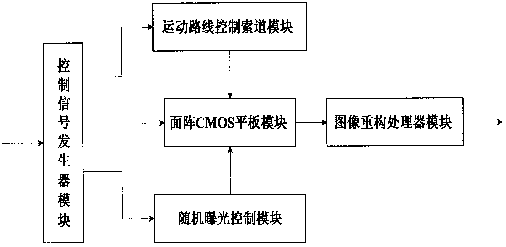
[0038] Refer to attached figure 1, The system of the present invention includes five modules: a control signal generator module, a motion route control cableway module, an area array CMOS panel module, a random exposure control module and an image reconstruction processor module, and each module is connected by a bus. Among them, the control signal generator module is used to generate the enable signal for controlling the motion route control cableway module, the exposure control module and the area array CMOS panel module to realize the driving of the system, and one output terminal of the control signal generator module is connected to the motion The input end of the route control cableway module, the second output end is connected to the input end of the random exposure control module, and the third output end is connected to the input end of the area array CMOS fla...


PUM


Abstract

The invention discloses a high-resolution imaging system and method based on a CMOS-TDI (Complementary Metal Oxide Semiconductor-Time Delay and Integration) mode, which mainly solves the problems in the prior art, such as low image obtaining efficiency and poor output image signal-to-noise ratio. The high-resolution imaging system comprises a signal control generator module, a movement route control cableway module, an area array CMOS plane module, a random exposure control module and an image reconstruction processor module. The high-resolution imaging method comprises the following steps of: 1, carrying out an initial operation; 2, carrying out push broom on s pixels by a prober; 3, generating a binary random sequence; 4, carrying out integral exposure by the prober; 5, carrying out internal transfer on photo-production charge pixels; 6, carrying out interline transfer on charges in a mask area; 7, judging whether a field scanning is completed or not; 8, outputting an observing value image; 9, optimizing and solving an L1-norm; and 10, obtaining a high-resolution image. The high-resolution imaging system and method provided by the invention have the advantages of simple circuit structure, low calculation complexity, high image obtaining efficiency and high output image signal-to-noise ratio.

Description

technical field [0001] The present invention belongs to the technical field of image processing, and further relates to an image compression coding based on Complementary Metal Oxide Semiconductor-Time Delay and Integration CMOS-TDI (Complementary Metal Oxide Semiconductor-Time Delay and Integration) mode in the technical field of high-resolution imaging Implement methods and build high-resolution imaging systems. The invention can realize high-resolution acquisition and reconstruction of images. Background technique [0002] High-resolution imaging has great demand in various fields, such as remote sensing monitoring, military reconnaissance, transportation and security monitoring, medical diagnosis and pattern recognition, etc. The spatial pixel resolution of conventional imaging depends on the pixel density of the detector. However, due to the limitations of processing technology and manufacturing materials, it is difficult and costly to obtain a high-resolution detecto...

Claims


Application Information

Patent Timeline
IPC IPC(8): H04N5/353H04N5/341H04N5/374
Inventor 石光明潘旋刘丹华董伟生高大化谢雪梅王晓甜
Owner XIDIAN UNIV
Why Eureka
Try Eureka