TFT (thin film transistor) array substrate

An array substrate and substrate technology, applied in optics, instruments, electrical components, etc., can solve problems such as unstable performance, low rate, and oxygen loss of metal oxides of TFT array substrates, so as to improve the overall etching speed, increase productivity, The effect of improving stability

Active Publication Date: 2012-08-22
BOE TECH GRP CO LTD
View PDF2 Cites 20 Cited by
  • Summary
  • Abstract
  • Description
  • Claims
  • Application Information

AI Technical Summary

Problems solved by technology

One side of the semiconductor layer is in contact with the etching barrier layer, and the other side is in contact with the gate insulating layer, wherein the etching barrier layer and the gate insulating layer are generally made of SiN x 、Al 2 o 3 or SiO x and other insulating materials, since the semiconductor layer is made of metal oxide materials, if the etch stop layer and the gate insulating layer are made of SiN x made, etch stop layer with gate insulating layer in SiN x It will capture the oxygen ions in the metal oxide that constitutes the semiconductor layer, causing the metal oxide in the semiconductor layer to lose oxygen, resulting in unstable performance of the TFT array substrate
[0005] In order to improve the stability of the TFT array substrate, the etch barrier layer and the gate insulating layer can also use Al 2 o 3 or SiO x made, but when dry etching is used, if Al 2 o 3 or SiO x To form the pattern of the etch barrier layer and the gate insulating layer, its etching rate is low, which is not conducive to mass production

Method used


Image

  • TFT (thin film transistor) array substrate
  • TFT (thin film transistor) array substrate
  • TFT (thin film transistor) array substrate

Examples


Embodiment 1

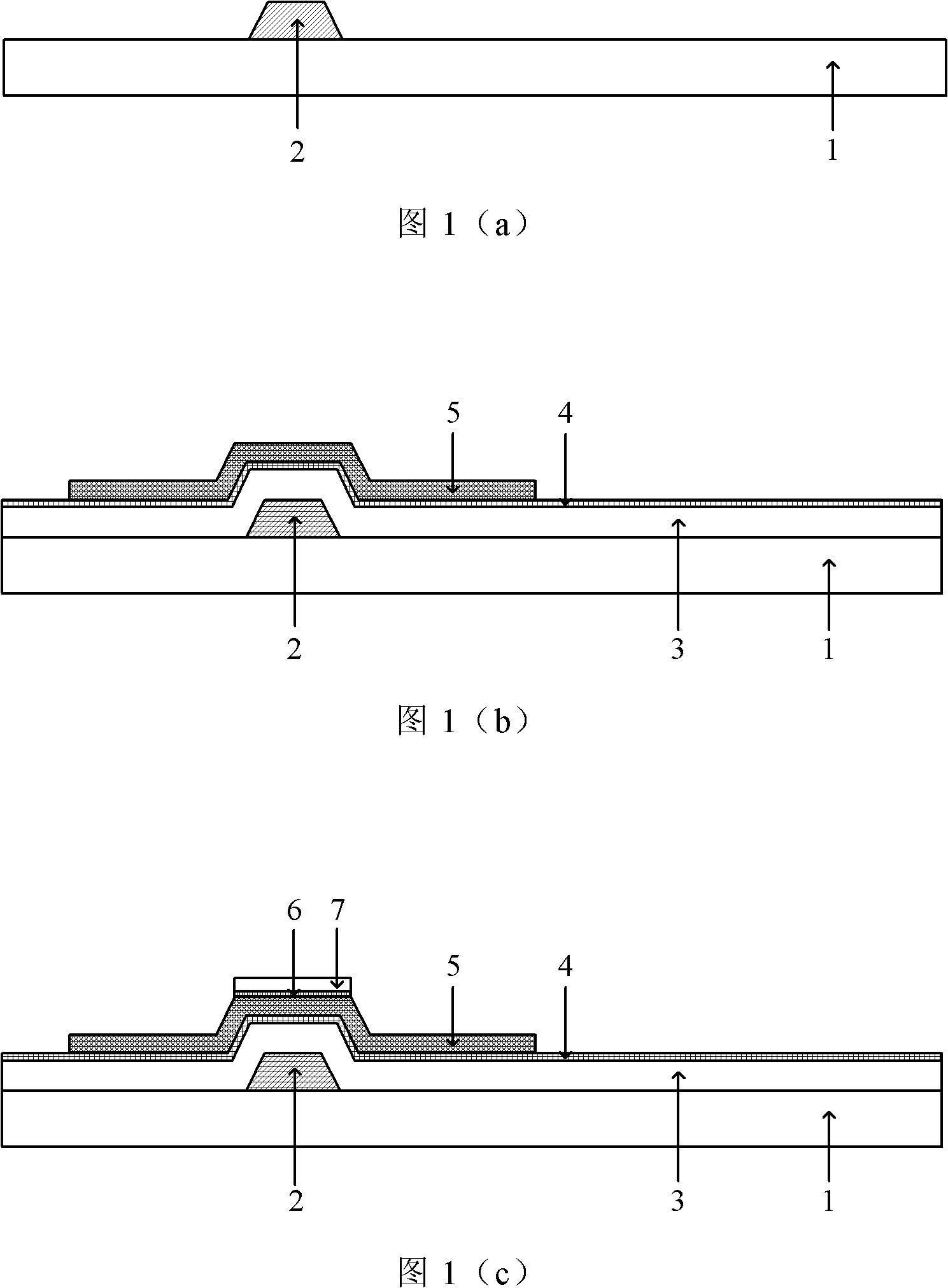
[0037] Such as figure 1As shown in (f), in this embodiment, the TFT array substrate includes: a substrate 1; a gate electrode 2 formed on the substrate; a gate insulating layer 3 covering the gate electrode 2 and extending to the substrate 1; The gate insulating protective layer 4 on the gate insulating layer 3; the semiconductor layer 5 formed on the gate insulating protective layer 4; the source electrode 8 and the drain electrode 9 formed on the semiconductor layer 5, the source electrode 8 and the drain electrode 9 A channel is provided between the drain electrodes 9; the etch stop protective layer 6 and the etch stop insulating layer 7 formed in the channel, the etch stop protective layer 6 is located under the etch stop insulating layer 7 and In contact with the semiconductor layer 5; the passivation layer 10, the passivation layer completely covers the source electrode 8, the etching stop insulating layer 7, the drain electrode 9 and the gate insulating protection layer...

Embodiment 2

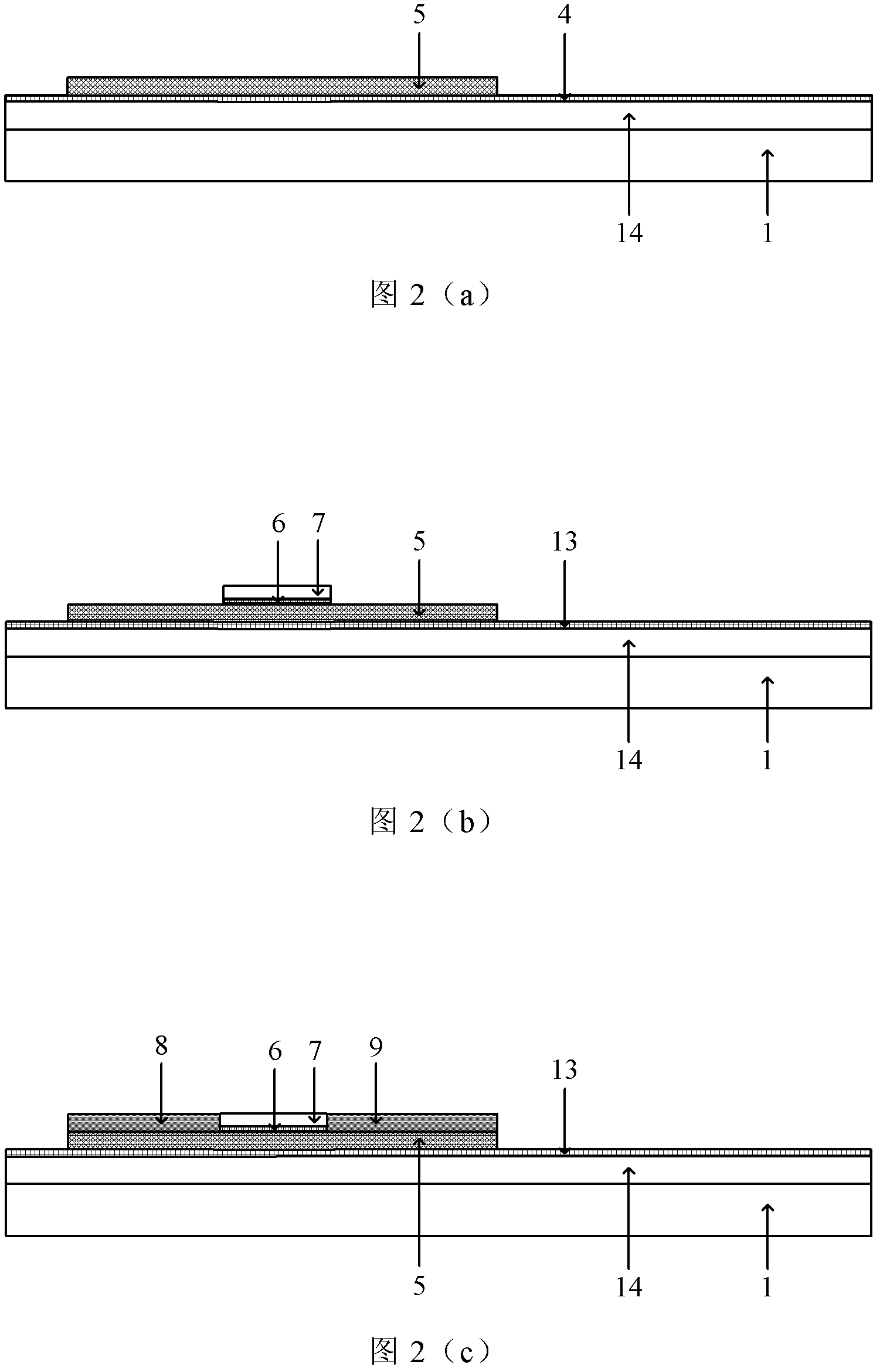
[0050] Such as figure 2 As shown in (f), in this embodiment, the TFT array substrate includes: a substrate 1; a modified insulating layer 14 covering the substrate; a modified insulating protection layer 13 covering the modified insulating layer 14; The semiconductor layer 5 on the semiconductor layer 5; the source electrode 8 and the drain electrode 9 formed on the semiconductor layer 5, and a channel is provided between the source electrode 8 and the drain electrode 9; the etching barrier protection formed in the channel layer 6 and an etch stop insulating layer 7, the etch stop protection layer 6 is located below the etch stop insulating layer 7 and is in contact with the semiconductor layer 5; a gate insulating layer 3, the gate insulating layer 3 connects the source electrode 8 , the etch stop insulating layer 7, the drain electrode 9 and the gate insulating protection layer 4 are completely covered, and the part of the gate insulating layer 3 covering the drain electrod...


PUM


Abstract

The invention provided a TFT (thin film transistor) array substrate, comprising a substrate (1) and a TFT, wherein the TFT comprises a gate electrode (2), a semiconductor layer (5), a source electrode (8) and a drain electrode (9), an adjacent layer of the semiconductor (5) is in a structure of a composite layer, the structure of the composite layer comprises a protective layer and an insulating layer, the protective layer can prevent the semiconductor layer (5) from losing oxygen, is made from an insulating material and is in contact with the semiconductor layer (5), and the insulating layer is made from an easily etching insulating material. The TFT array substrate can improve the stability of the TFT and is also suitable for large-batch production.

Description

technical field [0001] The invention belongs to the technical field of display manufacturing, and in particular relates to a TFT (Thin Film Transistor, thin film transistor technology) array substrate. Background technique [0002] With the development of display manufacturing technology, TFT-LCD (Thin Film Transistor Liquid Crystal Display) occupies a dominant position in the current flat panel display market due to its small size, low power consumption, and no radiation. [0003] The process of making a TFT array substrate in the prior art generally includes: sequentially depositing a gate metal film, a gate insulating film, a metal oxide film, a source-drain metal film, a passivation layer film, and a transparent conductive film on the substrate. Several photolithography processes sequentially form the patterns of the gate electrode, gate insulating layer, semiconductor layer, source electrode, drain electrode, passivation layer, and transparent pixel electrode. Etching ...

Claims


Application Information

Patent Timeline
Patent Type & Authority Applications(China)
IPC IPC(8): H01L27/02G02F1/1362G02F1/1368
CPCH01L29/4908H01L29/78606H01L29/66969H01L29/78603H01L29/7869H01L29/78693H01L27/1225H10K59/1213
Inventor 刘翔薛建设
Owner BOE TECH GRP CO LTD
Why Eureka
Try Eureka