

Super-junction vertical double-diffusion metal oxide semiconductor tube
A vertical double-diffusion and semiconductor tube technology, applied in semiconductor devices, electrical components, circuits, etc., can solve problems such as device damage, and achieve the effects of suppressing opening, improving reliability, and increasing area
- Summary
- Abstract
- Description
- Claims
- Application Information
AI Technical Summary
Problems solved by technology
Method used
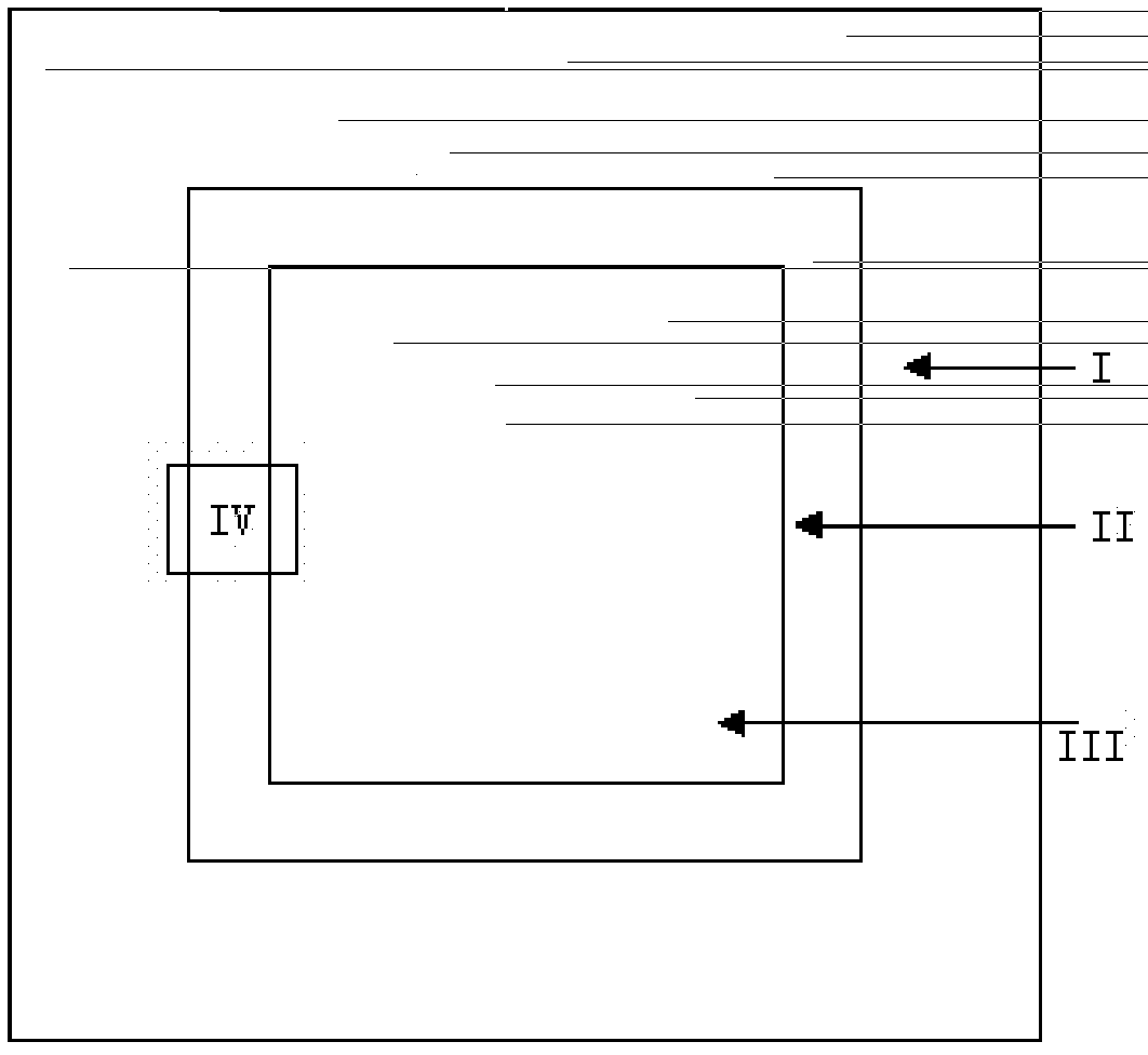
Image

Examples
Embodiment Construction
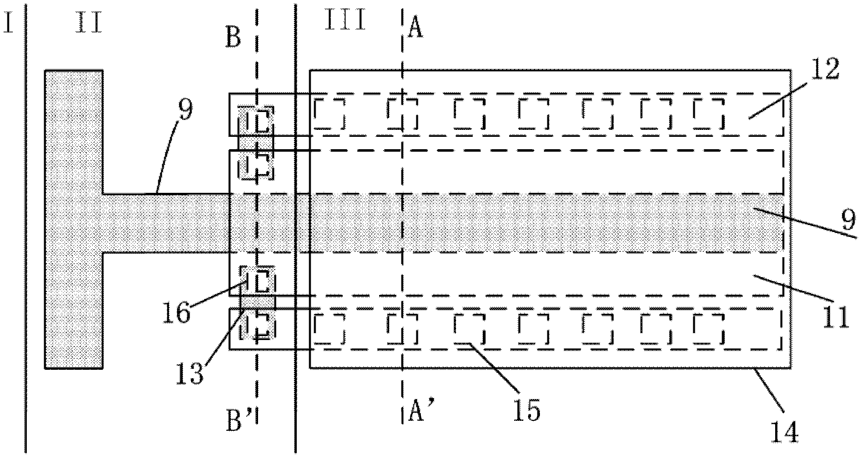
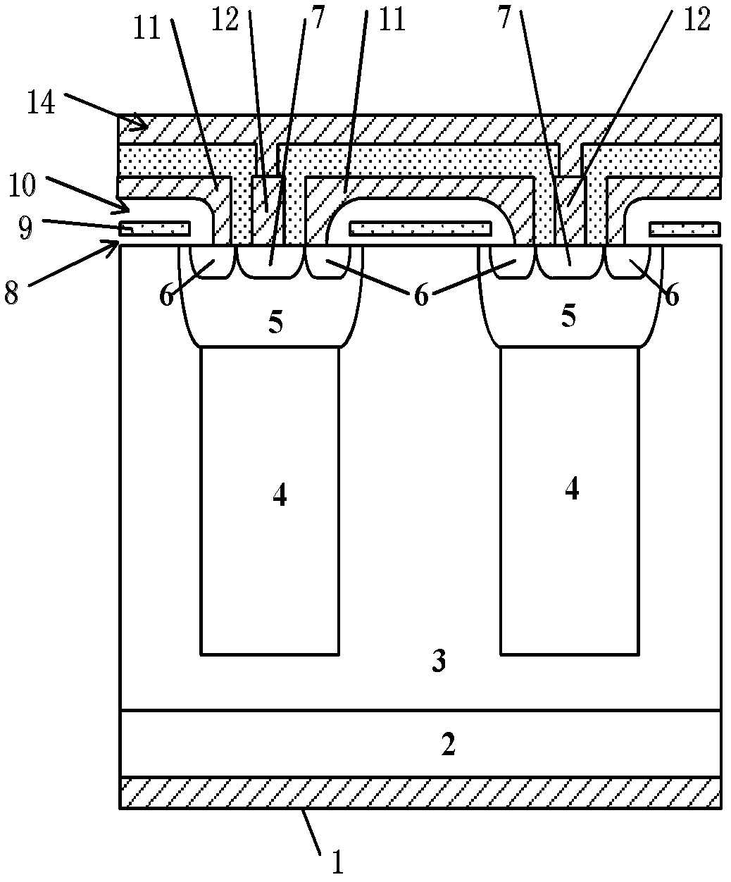
[0016] A super-junction vertical double-diffused metal oxide semiconductor tube, comprising: an N-type heavily doped silicon substrate 2 serving as a drain region, a drain metal 1 is arranged on the lower surface of the N-type heavily doped silicon substrate 2, An N-type doped silicon epitaxial layer 3 is arranged on the upper surface of the N-type heavily doped silicon substrate 2, and an intermittent and discontinuous P-type doped columnar semiconductor region 4 is arranged in the N-type doped silicon epitaxial layer 3. The P-type doped columnar semiconductor region 4 is provided with a first P-type doped semiconductor region 5, and the first P-type doped semiconductor region 5 is located in the N-type doped epitaxial layer 3, and in the first P-type doped semiconductor region 5 is provided with a second P-type heavily doped semiconductor contact region 7 and an N-type heavily doped semiconductor source region 6, and a gate oxide layer 8 is provided above the N-type doped sil...
PUM
 Abstract
Description
Claims
Application Information