

Surface treatment method of metal oxide and preparation method of thin film transistor
A thin-film transistor and surface treatment technology, which is applied in semiconductor/solid-state device manufacturing, semiconductor devices, electrical components, etc., can solve the problem of high contact resistance between metal oxides and electrodes, and achieve improved ohmic contact effect, increased concentration, and improved contact The effect of the characteristic
- Summary
- Abstract
- Description
- Claims
- Application Information
AI Technical Summary
Problems solved by technology
Method used
Image

Examples
Embodiment Construction
[0049] In order to enable those skilled in the art to better understand the technical solution of the present invention, the metal oxide surface treatment method and the preparation method of the thin film transistor provided by the present invention will be described in detail below with reference to the accompanying drawings.
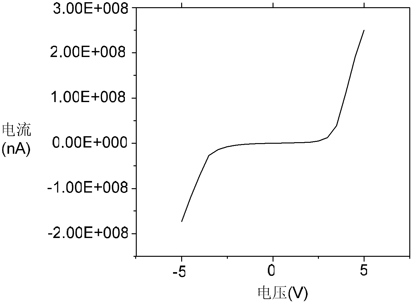
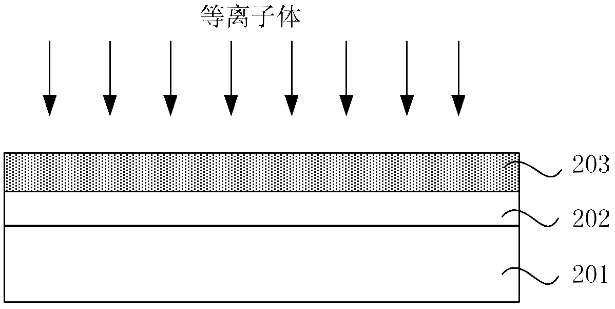
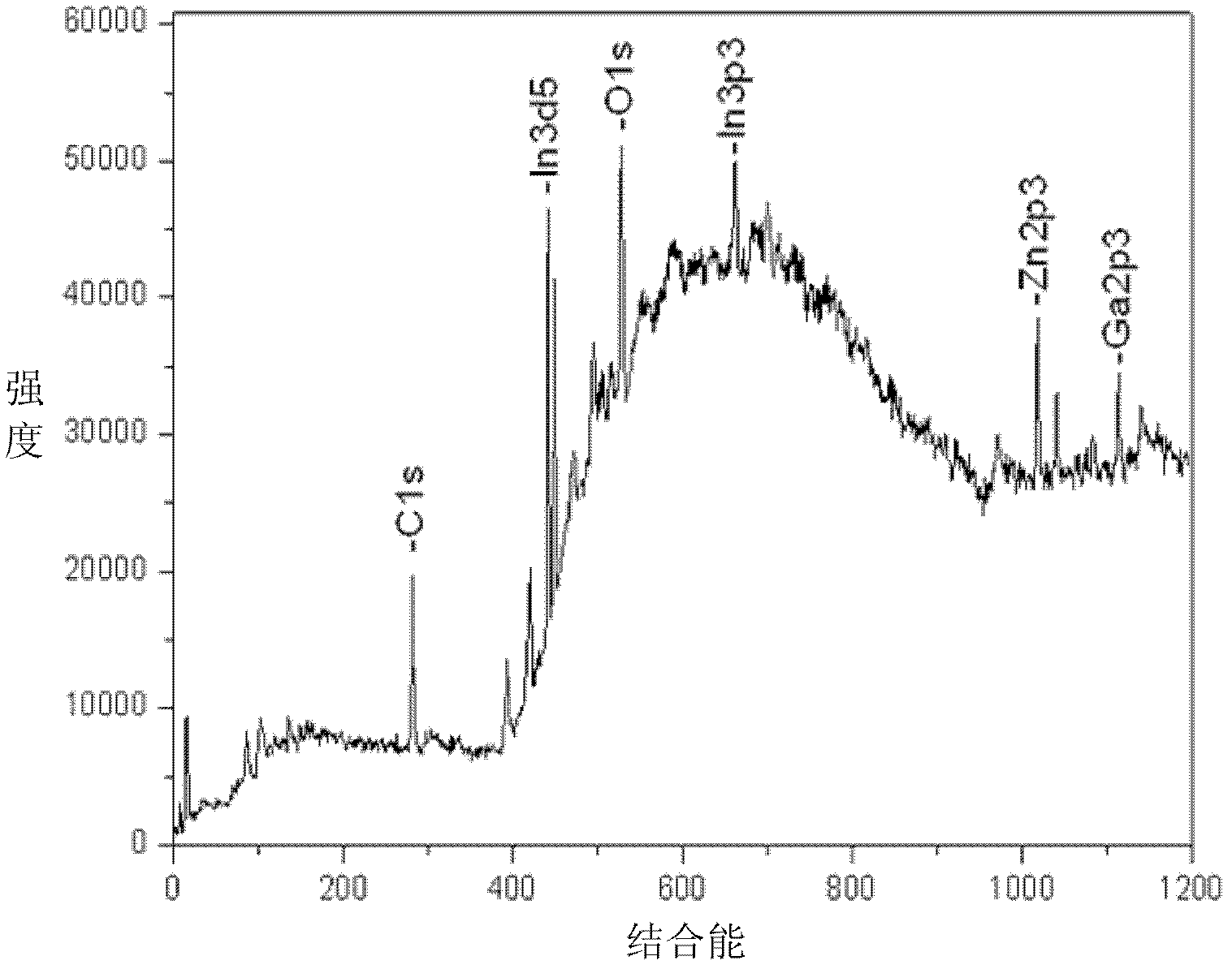
[0050] The device to be treated is treated with plasma, and the device to be treated may be a metal oxide or a product coated with a metal oxide. In this embodiment, the metal oxide is taken as an example to introduce the technical solution. figure 2 It is a schematic structural view of the first product in the first embodiment of the metal oxide surface treatment method of the present invention, image 3 It is the XPS spectrogram of the metal oxide processed in the present embodiment, Figure 4 It is the IV characteristic curve of the metal oxide treated in this example. Such as figure 2 As shown, a layer of insulating layer 202 is deposited on t...
PUM
 Abstract
Description
Claims
Application Information