Solid-state imaging device, electronic equipment, semiconductor device and manufacturing method of solid-state imaging device

A solid-state imaging device, semiconductor technology, applied in the direction of semiconductor devices, electrical solid-state devices, circuits, etc., can solve the problems of not providing reliability or product output rate, and achieve the effect of improving reliability and product output rate

Inactive Publication Date: 2012-08-29
SONY CORP
View PDF12 Cites 15 Cited by
  • Summary
  • Abstract
  • Description
  • Claims
  • Application Information

AI Technical Summary

Problems solved by technology

[0011] However, some semiconductor devices such as the above-mentioned solid-state imaging devices do not provide, for example, sufficiently high reliability or product yield

Method used


Image

  • Solid-state imaging device, electronic equipment, semiconductor device and manufacturing method of solid-state imaging device
  • Solid-state imaging device, electronic equipment, semiconductor device and manufacturing method of solid-state imaging device
  • Solid-state imaging device, electronic equipment, semiconductor device and manufacturing method of solid-state imaging device

Examples


Embodiment 1

[0037] 1. Example 1 (with annulus)

Embodiment 2

[0038] 2. Example 2 (without any annular ring)

[0039] 3. Other

[0040]

[0041] [A. Device structure]

[0042] (A-1) Structure of main parts of the camera

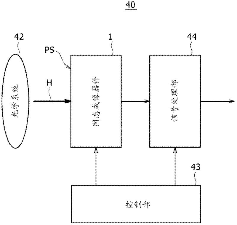
[0043] figure 1 It is a figure which shows the structure of the camera of Example 1.

[0044] Such as figure 1 As shown, the camera 40 includes a solid-state imaging device 1 , an optical system 42 , a control unit 43 and a signal processing unit 44 . These components will be described one by one.

[0045] The solid-state imaging device 1 receives incident light H entering as an object image via the optical system 42 with the imaging surface PS, and photoelectrically converts the received light, thereby generating signal charges. Here, the solid-state imaging device 1 is driven based on a control signal output from the control section 43 . Then, the signal charge is read and output as an electrical signal.

[0046] The optical system 42 includes optical members such as an imaging lens and a diaphragm, and is c...


PUM


Abstract

The invention discloses a solid-state imaging device, an electronic equipment, a semiconductor device and a manufacturing method of the solid-state imaging device.Disclosed herein is a solid-state imaging device including: a sensor element having a plurality of pixels each having a photoelectric conversion section; and a logic element attached to the sensor element in such a manner as to be stacked on the sensor element face-to-face and provided with a pad electrode. In a stacked body of the sensor and logic elements, a pad opening is provided above the top surface of the pad electrode facing the sensor element, and a pad periphery guard ring is provided to surround the side portion of the pad opening. The pad periphery guard ring is formed by integrally filling, on the side of the pad opening, an entire trench that is at least as deep as the pad opening with a metal material.

Description

technical field [0001] The present technology relates to a solid-state imaging device, an electronic device, a semiconductor device, and a method of manufacturing the solid-state imaging device. Background technique [0002] Electronic equipment such as digital camcorders and digital cameras include solid-state imaging devices. Among the solid-state imaging devices are a CMOS (Complementary Metal Oxide Semiconductor) image sensor and a CCD (Charge Coupled Device) image sensor. [0003] A solid-state imaging device has a plurality of pixels arranged on the surface of a semiconductor substrate. A photoelectric conversion unit is provided in each pixel. The photoelectric conversion section is, for example, a photodiode, and receives incident light entering via an external optical system with its light receiving surface to photoelectrically convert the received light, thereby generating signal charges. [0004] In a solid-state imaging device, pixels of a CMOS image sensor ea...

Claims


Application Information

Patent Timeline
Patent Type & Authority Applications(China)
IPC IPC(8): H01L27/146
CPCH01L27/14618H01L27/14621H01L27/14627H01L27/14636H01L27/1464H01L27/14683H01L2924/0002H01L2924/00
Inventor 西泽贤一
Owner SONY CORP
Why Eureka
Try Eureka