CMOS (Complementary Metal Oxide Semiconductor) image sensor and production method thereof
A technology of an image sensor and a manufacturing method, applied in the field of semiconductors, can solve the problems of unsatisfactory imaging quality and decreased light absorption efficiency, and achieve the effects of low power consumption, improved absorption efficiency, and enhanced absorption
- Summary
- Abstract
- Description
- Claims
- Application Information
AI Technical Summary
Problems solved by technology
Method used
Image

Examples
Embodiment 1
[0059] Such as Figure 2a to Figure 2c As shown, the present invention provides a kind of CMOS image sensor fabrication method, and this method at least comprises the following steps:
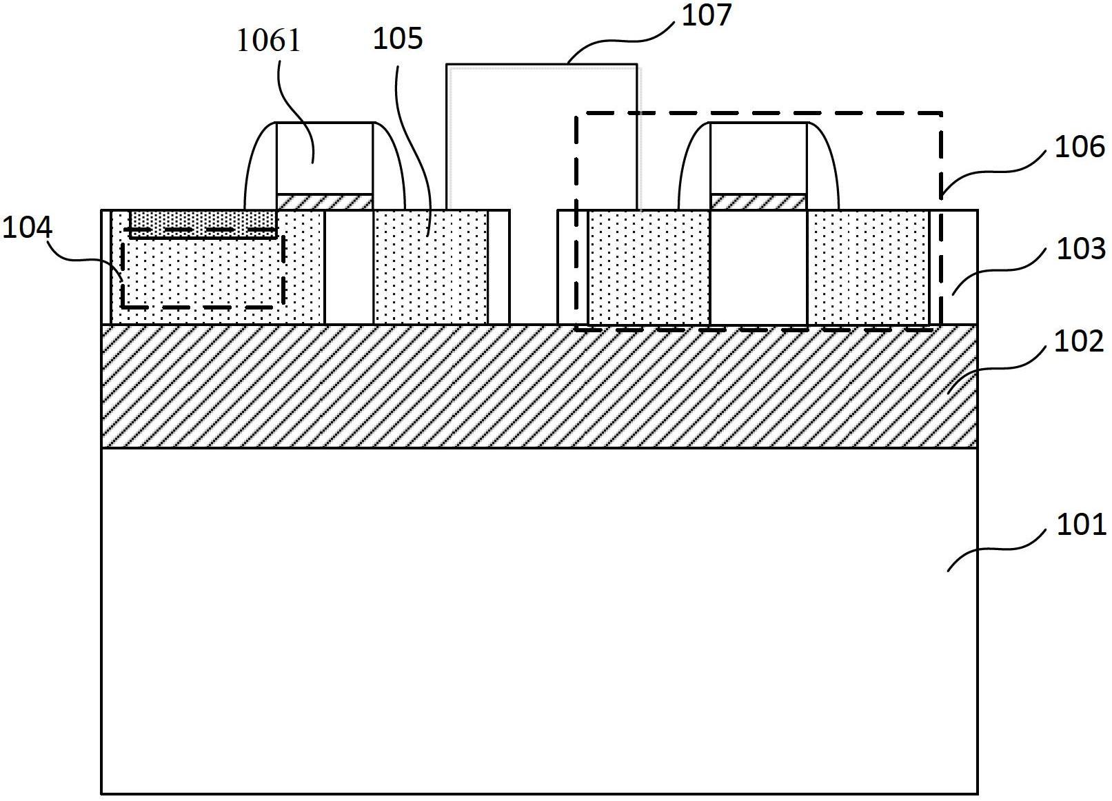
[0060] Such as Figure 2a As shown, step 1) is first performed to provide a semiconductor substrate, the semiconductor substrate is a silicon substrate or has a supporting substrate 201, an insulating buried layer 202 on the supporting substrate 201, and a The semiconductor substrate of the top semiconductor layer 203 above the insulating buried layer 202; the photosensitive device 204 and the pixel readout circuit 206 are fabricated in the semiconductor substrate, and the isolation structure 208 between adjacent devices is formed, wherein, when When the semiconductor substrate is a semiconductor substrate with an insulating buried layer, the photosensitive device 204 , the pixel readout circuit 206 and the isolation structure 208 are all fabricated in the top semiconductor layer 203 . Specif...
Embodiment 2
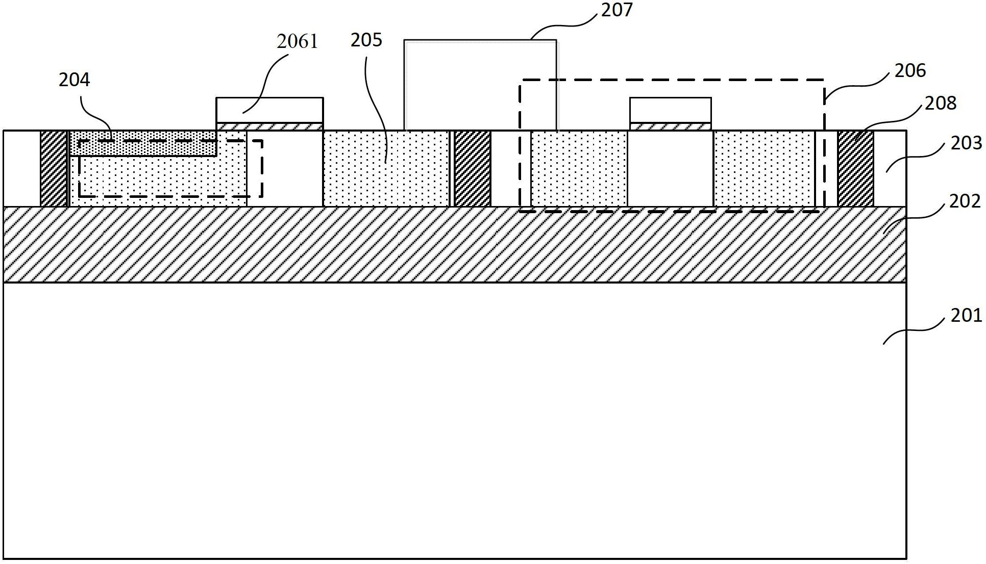
[0077] Such as Figures 3a to 3b As shown, the present invention provides a CMOS image sensor, the image sensor at least includes: a semiconductor substrate, a photosensitive device 304, a pixel readout circuit 306, an isolation structure 307, a dielectric layer (not shown) and metal wiring (not shown) shown), nano metal particle layer 308.
[0078] The semiconductor substrate is a silicon substrate or a semiconductor substrate having a supporting substrate 301, an insulating buried layer 302 on the supporting substrate 301, and a top semiconductor layer 303 on the insulating buried layer 302 Bottom; the material of the top semiconductor layer 303 is a semiconductor material used to make semiconductor devices, including at least any one of silicon, strained silicon, germanium and silicon germanium; the insulating buried layer 302 is a single-layer structure or stacked layers structure, wherein the single-layer structure or the material of each layer in the stacked structure i...
PUM
| Property | Measurement | Unit |
|---|---|---|
| Diameter | aaaaa | aaaaa |
| Diameter | aaaaa | aaaaa |
Abstract
Description
Claims
Application Information
 - Generate Ideas
- Intellectual Property
- Life Sciences
- Materials
- Tech Scout
- Unparalleled Data Quality
- Higher Quality Content
- 60% Fewer Hallucinations
Browse by: Latest US Patents, China's latest patents, Technical Efficacy Thesaurus, Application Domain, Technology Topic, Popular Technical Reports.
© 2025 PatSnap. All rights reserved.Legal|Privacy policy|Modern Slavery Act Transparency Statement|Sitemap|About US| Contact US: help@patsnap.com