Method for preparing structured graphene by reaction of SiC and Cl2 based on Ni film annealing

An annealing and fossilization technology, applied in the field of microelectronics, can solve the problems of reduced electron mobility of graphene, expensive single crystal SiC, affecting device performance, etc., and achieves the effect of easy control of thickness, fast reaction rate, and guaranteed device performance

Inactive Publication Date: 2012-09-19
XIDIAN UNIV
View PDF2 Cites 5 Cited by
  • Summary
  • Abstract
  • Description
  • Claims
  • Application Information

AI Technical Summary

Problems solved by technology

However, the single crystal SiC used in the thermal decomposition of SiC is very expensive, and the grown graphene is distributed in an island shape, with many pores and uneven layers, and the photolithography and dry etching process will make the graphene Electron mobility decreases, which affects device performance

Method used


Image

  • Method for preparing structured graphene by reaction of SiC and Cl2 based on Ni film annealing
  • Method for preparing structured graphene by reaction of SiC and Cl2 based on Ni film annealing
  • Method for preparing structured graphene by reaction of SiC and Cl2 based on Ni film annealing

Examples


Embodiment 1

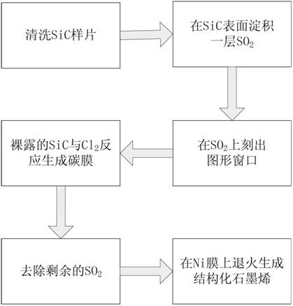
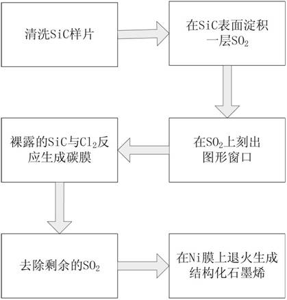
[0026] Step 1: Wash the 6H-SiC sample to remove surface contamination.

[0027] (1.1) Use NH for 6H-SiC substrate 4 OH+H 2 o 2 Soak the sample in the reagent for 10 minutes, take it out and dry it to remove the organic residue on the surface of the sample;

[0028] (1.2) Use HCl+H on the 6H-SiC sample after removing the surface organic residues 2 o 2 The reagent soaked the sample for 10 minutes, took it out and dried it to remove ionic contamination.

[0029] Step 2: Deposit a layer of SiO on the surface of the 6H-SiC sample 2 .

[0030] (2.1) Put the cleaned 6H-SiC sample into the PECVD system, adjust the internal pressure of the system to 3.0Pa, adjust the RF power to 100W, and adjust the temperature to 150°C;

[0031] (2.2) Introduce SiH with flow rates of 30sccm, 60sccm and 200sccm into the system 4 , N 2 O and N 2 , the duration is 20min, making SiH 4 and N 2 O reaction, deposit a layer of 0.4 μm thick SiO on the surface of 6H-SiC sample 2 mask layer.

[003...

Embodiment 2

[0051] Step 1: Clean the 4H-SiC sample to remove surface pollutants.

[0052] For 4H-SiC substrates, use NH first 4 OH+H 2 o 2Soak the sample in the reagent for 10 minutes, take it out and dry it to remove the organic residue on the surface of the sample; then use HCl+H 2 o 2 The reagent soaked the sample for 10 minutes, took it out and dried it to remove ionic contamination.

[0053] Step 2: Deposit a layer of SiO on the surface of the 4H-SiC sample 2 .

[0054] Put the cleaned 4H-SiC sample into the PECVD system, adjust the internal pressure of the system to 3.0Pa, adjust the RF power to 100W, and adjust the temperature to 150°C; feed SiH with flow rates of 30sccm, 60sccm and 200sccm into the system 4 , N 2 O and N 2 , the duration is 75min, making SiH 4 and N 2 O reaction, deposit a layer of 0.8 μm thick SiO on the surface of 4H-SiC sample 2 .

[0055] Step 3: On SiO 2 The graphics window is engraved on the layer.

[0056] In SiO 2 Spin-coat a layer of photor...

Embodiment 3

[0067] Step A: Clean the surface of the 6H-SiC substrate, that is, use NH 4 OH+H 2 o 2 Soak the sample in the reagent for 10 minutes, take it out and dry it to remove the organic residue on the surface of the sample; then use HCl+H 2 o 2 The reagent soaked the sample for 10 minutes, took it out and dried it to remove ionic contamination.

[0068] Step B: Put the cleaned 6H-SiC sample into the PECVD system, adjust the internal pressure of the system to 3.0Pa, adjust the radio frequency power to 100W, and adjust the temperature to 150°C; the flow rates into the system are respectively 30sccm, 60sccm and 200 sccm of SiH 4 , N 2 O and N 2 , the duration is 100min, so that SiH 4 and N 2 O reaction, a layer of 1.2 μm thick SiO was deposited on the surface of the 6H-SiC sample 2 .

[0069] Step C: Same as Step 3 of Example 1.

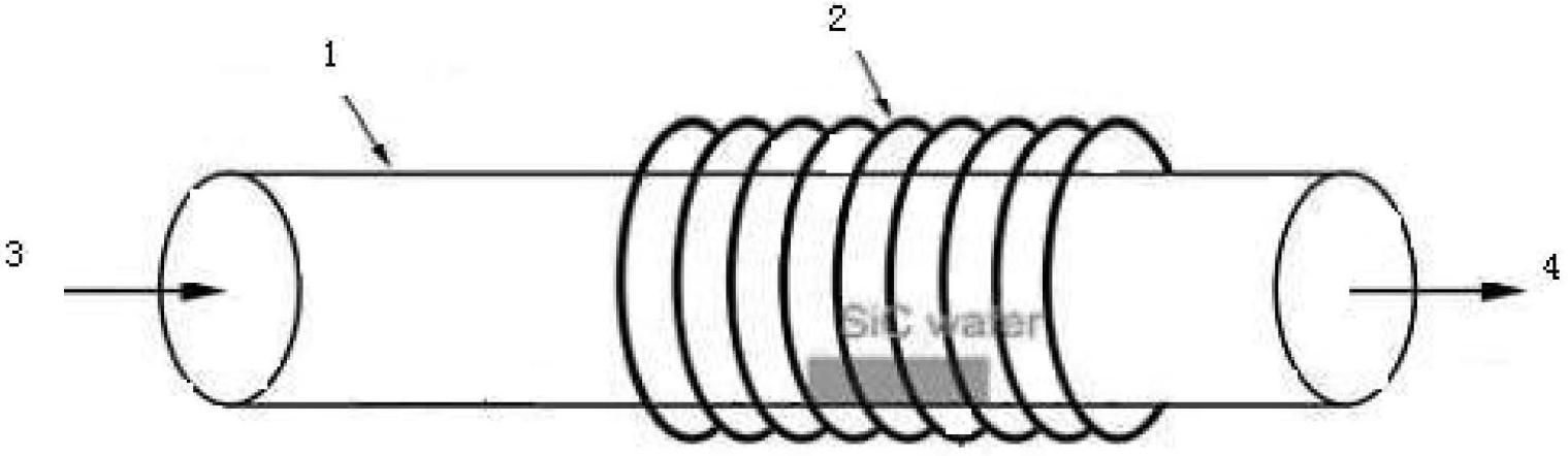
[0070] Step D: place the sample piece after opening the window in the quartz tube 1, and place the quartz tube in the resistance furnace 2; feed th...


PUM


Abstract

The invention discloses a method for preparing structured graphene by reaction of SiC and Cl2 based on Ni film annealing, mainly aiming at solving the problems that the graphene prepared by the prior art is not smooth in surface, and is poor in continuity and uneven in the number of layers. The realization process of the method comprises the steps of: carrying out standard cleaning on a SiC sample piece; depositing a layer of SiO2 on the surface of the cleaned SiC sample piece, and carving a graphic window; after the graphic window is formed, putting the sample piece into a quartz tube, and generating a carbon film at the temperature of 700-1100 DEG C; then, putting the generated carbon film sample piece into a buffer hydrofluoric acid solution, and removing the SiO2 outside the window; after that, depositing a layer of Ni film on another Si sample piece by electron beams; arranging the carbon film sample piece without SiO2 on the Ni film, and arranging in Ar gas; and carrying out annealing at 900-1100 DEG C for 10-30minutes, and generating the structured graphene. The method has the advantages of being simple in technology, high in safety, smooth in the surface of the generated structured graphene, good in continuity of the generated structured grapheme and low in porosity of the generated structured graphene, thus being used for making a microelectronic device.

Description

technical field [0001] The invention belongs to the technical field of microelectronics, and relates to a semiconductor thin film material and a preparation method thereof, specifically SiC and Cl based on Ni film annealing. 2 Method for preparing structured graphene by reaction. technical background [0002] Graphene appeared in the laboratory in 2004. At that time, two scientists, Andre Gem and Kostya Novoselov, from the University of Manchester in the United Kingdom discovered that they could obtain more and more graphene in a very simple way. thinner and thinner graphite flakes. They peeled off the graphite flakes from the graphite, then glued the two sides of the flakes to a special adhesive tape, and when the tape was torn off, the graphite flakes could be split in two. Repeatedly doing this, the flakes got thinner and thinner, and eventually, they got a flake made of just one layer of carbon atoms, which is graphene. Since then, new methods of preparing graphene ha...

Claims


Application Information

Patent Timeline
Patent Type & Authority Applications(China)
IPC IPC(8): C01B31/04C01B32/188
Inventor 郭辉邓鹏飞张玉明张克基雷天民张凤祁
Owner XIDIAN UNIV
Why Eureka
Try Eureka