Automatic detection method of solar silicon chip colors based on machine vision

A technology of machine vision and automatic detection, which is applied in the direction of color measurement devices, optical testing flaws/defects, etc., can solve problems such as unreachable, no substantial progress in detection methods, instability, etc., and achieve the effect of automation

Inactive Publication Date: 2012-09-19
JIANGNAN UNIV
View PDF3 Cites 20 Cited by
  • Summary
  • Abstract
  • Description
  • Claims
  • Application Information

AI Technical Summary

Problems solved by technology

Due to color defects on the surface of silicon wafers (including yellow, red, white, small white spots, roller marks, fingerprint stains, boat pollution stains, chemical residue stains, metaphosphoric acid stains, aluminum film and The diversity and complexity of the process dots, etc.) have led to no subst

Method used


Image

  • Automatic detection method of solar silicon chip colors based on machine vision
  • Automatic detection method of solar silicon chip colors based on machine vision
  • Automatic detection method of solar silicon chip colors based on machine vision

Examples


Embodiment Construction

[0018] The specific embodiments of the present invention will be further described below in conjunction with the accompanying drawings.

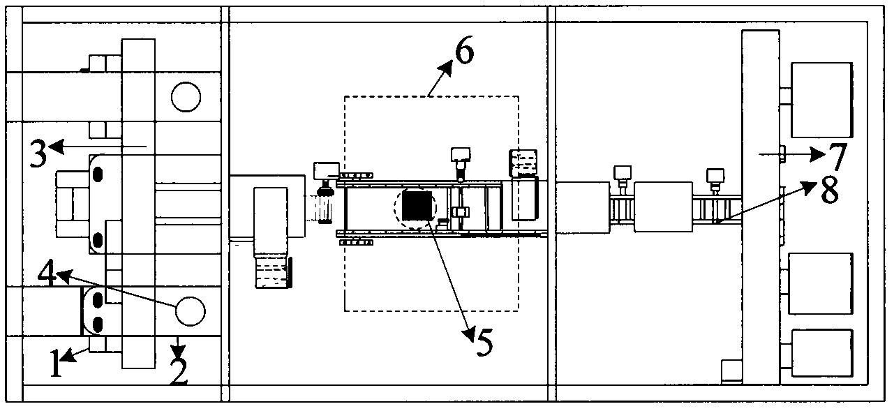
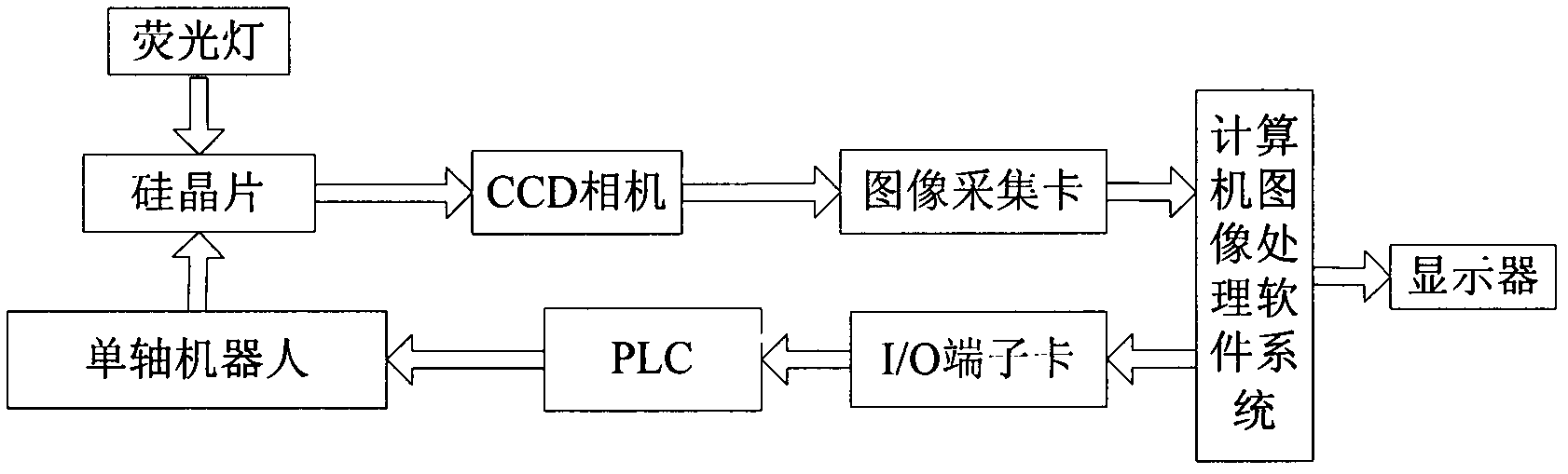
[0019] Automatic detection process: Manually place the material box full of silicon wafers at the designated position; press the device start button; the cylinder pulls the material box to the upper material position; the silicon wafer is lifted by the servo action, and the silicon wafer is moved up; the photoelectric switch is sensed; Lift to the right position; move the module horizontally to the grabbing position; the suction cup works; position; the cylinder moves down; the suction cup stops sucking; the silicon wafer is placed on the transmission belt line; the silicon wafer is translated to the camera inspection station; the camera takes pictures for inspection; the inspection is completed; position; the sorting module, cylinder, and suction cups act to sort silicon wafers into the designated tray; the equipment operates in a cycle. T...


PUM


Abstract

The invention relates to the machine vision detection field, and discloses a method and a device for detecting surface color defects of solar silicon chips through the machine vision technology. The detection object is distribution information of the surface colors of the silicon chips after a process of plasma enhanced chemical vapor deposition (PECVD). The classifying scheme includes using an image filtering technique, a color image segmentation technique, a color image hue, saturation, and lightness (HIS) spatial analysis technique and the like for processing and analyzing collected images; extracting feature information of the images; classifying the silicon chips into good silicon chips and defect silicon chips according to surface quality after training and testing of the information through a mode identifying method which combines a support vector machine with an improved gravitational search algorithm; sending a classifying result to an executive mechanism and controlling a uniaxial robot to take out the defect silicon chips. According to the method and the device, mechanism is simple, maintenance and operation are facilitated, and detecting requirements can be satisfied.

Description

technical field [0001] The invention relates to an automatic detection technology of solar silicon wafer color based on machine vision, which is used for automatic online detection of unqualified color defects produced on the surface after the plasma enhanced chemical vapor deposition (Plasma Enhanced Chemical Vapor Deposition, referred to as PECVD) process silicon wafer. Background technique [0002] Silicon wafers are the core material of solar cells, and their quality directly determines the performance of solar cells. Therefore, silicon wafers with color defects must be rejected during inspection. Due to color defects on the surface of silicon wafers (including yellow, red, white, small white spots, roller marks, fingerprint stains, boat pollution stains, chemical residue stains, metaphosphoric acid stains, aluminum film and The diversity and complexity of the process dots, etc.) have led to no substantial progress in the research on its detection methods. At present, m...

Claims


Application Information

Patent Timeline
IPC IPC(8): G01J3/46G01N21/95
Inventor 潘丰李春龙张相胜
Owner JIANGNAN UNIV
Why Eureka
Try Eureka