Manufacture method fro transparent electrodes

A manufacturing method and technology for transparent electrodes, which are applied in cable/conductor manufacturing, circuits, electrical components, etc., can solve the problems of reduced transparency of graphene, blocking light, and difficulty in making transparent electrodes.

Inactive Publication Date: 2012-09-19
RITEDIA CORPORATION
View PDF3 Cites 8 Cited by
  • Summary
  • Abstract
  • Description
  • Claims
  • Application Information

AI Technical Summary

Problems solved by technology

However, because copper is almost insoluble in carbon, the carbon decomposed by carbon-containing gas is deposited on the surface of copper, and only one or two layers of graphene can grow. In addition, there are many defects in it, so the conductivity is low
If carbon-containing gas is deposited on the surface of a soluble metal (such as nickel, cobalt, iron, palladium, or platinum) by vapor deposition, due to the high solubility of carbon, the number of graphene layers precipitated can exceed 100 layers, or even Tens of thousands of layers, so that the transparency of graphene is greatly reduced, making it difficult for light to pass through, and the light transmittance is not good.
[0007] Furthermore, after graphene is cooled from high temperature (1000°C), graphene hardly shrinks, but the shrinkage rate of the attached metal is very large (up to 1%), so the graphene attached to the metal will be compressed and wrinkled, Therefore, the light shining on the graphene will be absorbed in the creases and generate heat
In addition, the nucleation direction of graphene on the metal is different, so that the crystal lattice direction is staggered after the crystal grows, so that a lot of defects are formed at the junction of the grain boundary, including plug-in rows, pentagonal rings, heptagons...etc. , the carbon atoms that do not belong to the hexagonal ring will block the light and reduce the current, so it is difficult to make a transparent electrode

Method used


Image

  • Manufacture method fro transparent electrodes
  • Manufacture method fro transparent electrodes
  • Manufacture method fro transparent electrodes

Examples


Embodiment 1

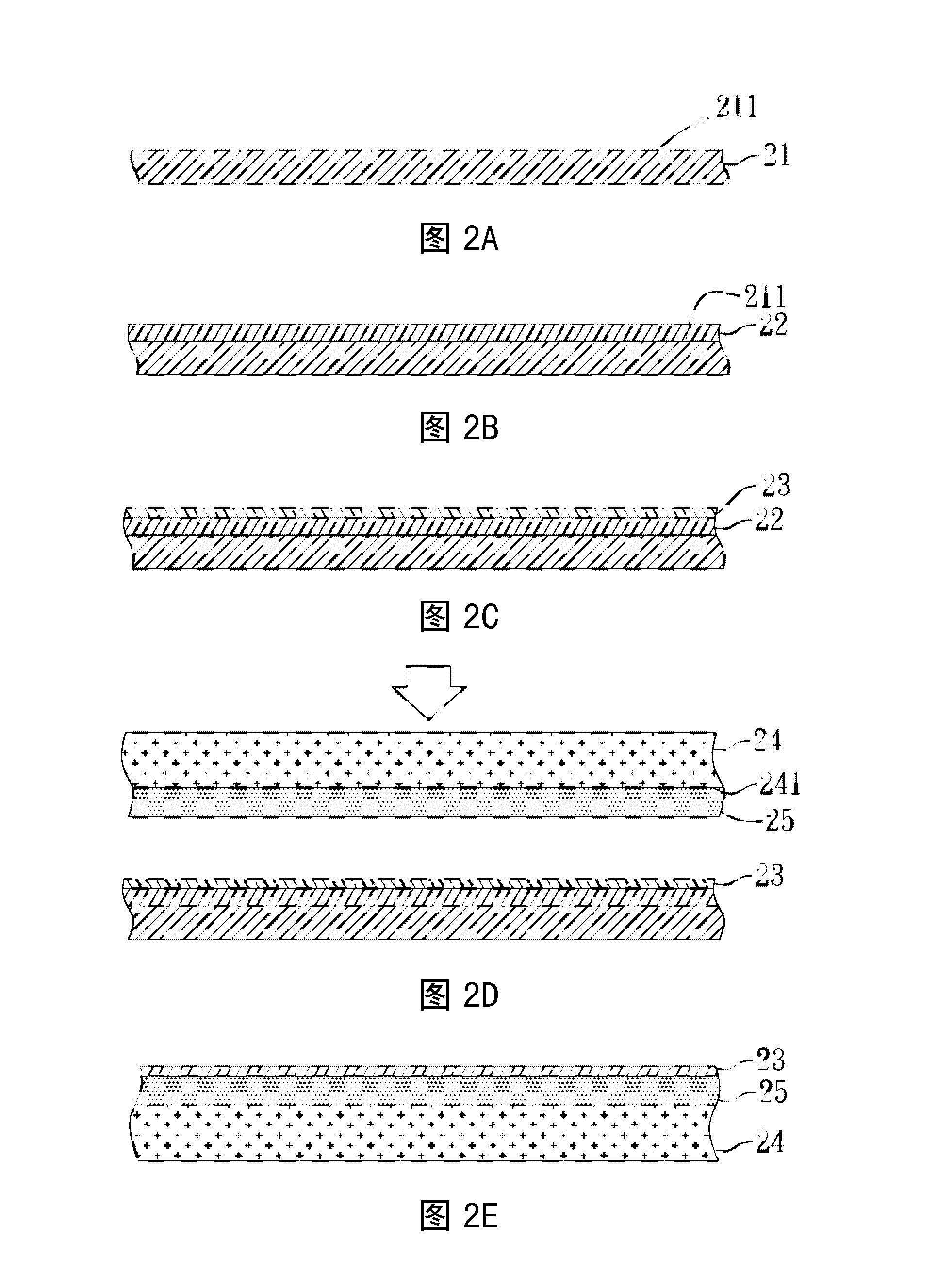
[0040] For a manufacturing method of a transparent electrode of this embodiment, please refer to Figure 2A to Figure 2E . Figure 2A to Figure 2E It is a schematic diagram of a manufacturing method of a transparent electrode of the present invention.

[0041] Please see first Figure 2A , at first provide a substrate 21, is to have a first surface 211, then, please refer to Figure 2B , form a carbon solvent layer 22 on the first surface 211 on the substrate 21, the method of forming the carbon solvent layer 22 is chemical vapor deposition, then, as Figure 2C Therefore, a carbon source (not shown in the figure) is provided, and the carbon source is a carbon-containing gas, and the carbon-containing gas is heated to form a plurality of graphene layers 23 on the carbon solvent layer 22 .

[0042] In the manufacturing method of a transparent electrode of this embodiment, the above-mentioned substrate is not limited to the substrate made of copper used in this embodiment, and...


PUM

PropertyMeasurementUnit
thicknessaaaaaaaaaa
transmittivityaaaaaaaaaa

Abstract

The invention provides a manufacture method for transparent electrodes, comprising steps of: (A) providing a carbon-insoluble substrate provided with a first surface; (B) forming a carbon solvent layer on the first surface of the substrate; (C) providing a carbon source; and (D) forming a plurality of graphene layers on the carbon solvent layer. Wherein the thickness of graphene layers is controlled by the carbon solvent layer, the carbon source is supplied by a carbon-containing gas, and is used for controlling the growth rate of the graphene layers.

Description

technical field [0001] The invention relates to a method for manufacturing a transparent electrode, in particular to a method for making a transparent electrode made of graphene, which can manufacture a graphene transparent electrode with high conductivity and high transparency. Background technique [0002] The Dutch scholar Andre Geim and the British Konstantin Novoselov became the winners of the 2010 Nobel Prize in Physics for their discovery of graphene, the thinnest material in the world. [0003] Graphene has a wide range of applications, such as IC circuits (replacing copper wires), transparent electrodes (replacing ITO), lithium-ion batteries (replacing anodes), supercapacitors (replacing graphite for electricity storage), super tires (replacing strengthened graphite Tim Ji), biological chip (replacing silicon), graphene diaphragm and so on. [0004] The use of graphene to make transparent electrodes is one of the most popular applications of graphene. South Korea'...

Claims


Application Information

Patent Timeline
Patent Type & Authority Applications(China)
IPC IPC(8): H01B13/00H01B5/14B32B9/00
CPCG02F1/1343H01L29/458H01L29/1606H01L51/442H01L29/45G02F1/13439H01L51/5203H01L31/022466H01L29/40H01L2933/0016G02F2203/01H01L29/4908H01L29/786H01L33/42H01L51/5206H10K30/82H10K50/81H10K50/816
Inventor 宋健民
Owner RITEDIA CORPORATION
Why Eureka
Try Eureka