Radiating structure for single chip package and system-in-package

A technology of system-level packaging and heat dissipation structure, which is applied in cooling/ventilation/heating transformation, instruments, sustainable buildings, etc., can solve problems such as cost increase, achieve the effect of increasing channels, reducing system hot spots, and improving heat dissipation efficiency

Inactive Publication Date: 2012-09-19
INST OF MICROELECTRONICS CHINESE ACAD OF SCI
View PDF9 Cites 16 Cited by
  • Summary
  • Abstract
  • Description
  • Claims
  • Application Information

AI Technical Summary

Problems solved by technology

The main problem of this method is that it needs to design a special plastic sealing mold and adopt advanced new plastic sealing equipment, which will greatly increase the cost

Method used


Image

  • Radiating structure for single chip package and system-in-package
  • Radiating structure for single chip package and system-in-package
  • Radiating structure for single chip package and system-in-package

Examples


Embodiment Construction

[0076] In order to make the object, technical solution and advantages of the present invention clearer, the present invention will be described in further detail below in conjunction with specific embodiments and with reference to the accompanying drawings.

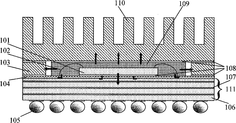
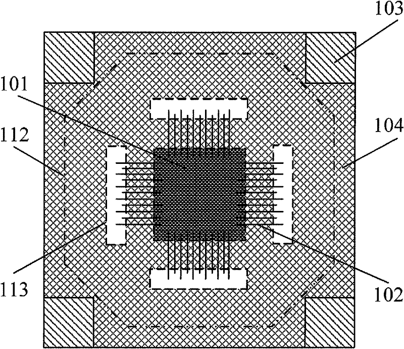
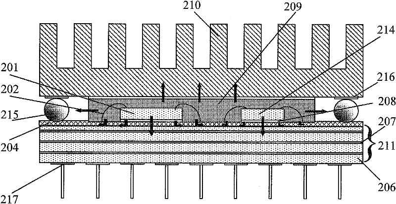
[0077] The present invention closely contacts the large-area heat sink structure directly below the bare chip, conducts more heat to the heat sink, and directly takes away the heat through the system air cooling, reducing system hot spots caused by conduction to the PCB through the substrate. Provides a third heat conduction direction for connecting heat sinks other than the top and surroundings for chip or module heat dissipation. In terms of mechanism, the heat conduction path, area and heat radiation are increased, and the heat dissipation efficiency is improved. It can also be flexibly combined with other heat dissipation methods to improve the overall heat dissipation effect.

[0078] Based on the above realization ...


PUM


Abstract

The invention discloses a radiating structure for a single chip package and a system-in-package. The radiating structure comprises a radiating fin, supporting structures and a radiator, the radiating fin is positioned between a substrate and a chip and used for absorbing heat generated by the chip, the upper surface of the radiating fin directly contacts with the lower surface of the chip, and the lower surface of the radiating fin directly contacts with the upper surface of the substrate; the supporting structures are positioned at four ends of the radiating fin, one end of each supporting structure directly contacts with the upper surface of the radiating fin, the other end of each supporting structure directly contacts with the lower surface of the radiator, and the supporting structures are used for absorbing heat which is generated by the chip and transmitted to the radiator via the radiating fin; and the radiator is positioned above the chip and used for dissipating heat transmitted from the radiating fin and the supporting structures. The radiating structure for the single chip package and the system-in-package is simple is implemented easily, can be conveniently used with other radiating methods, and has an excellent application prospect in terms of solving the problem of radiating for the single chip package and the system-in-package, particularly chips or systems-in-package with high power consumption.

Description

technical field [0001] The invention relates to the technical field of microelectronic packaging, relates to the field of single-chip packaging, two-dimensional or three-dimensional multi-chip system-in-package, and specifically relates to a heat dissipation structure for single-chip packaging and system-in-package (SiP). Background technique [0002] With the development of high-speed, high-density, and high-performance microelectronic chips, thermal management has become a very important issue in microsystem packaging. The problem of heat dissipation in integrated circuits is very important in many applications. The power consumption of a high-performance single chip represented by a CPU has exceeded 100W, and heat dissipation will directly affect the design performance of the chip. In order to meet people's needs for miniaturization, multi-function, and environmental protection of electronic products, the new heterogeneous integration technology System-in-Package (SiP) is...

Claims


Application Information

Patent Timeline
Patent Type & Authority Applications(China)
IPC IPC(8): H01L23/367H01L23/373H01L23/467H05K7/20G06F1/20
CPCH01L2924/0002H01L2924/15311Y02B60/1275H01L2224/48091H01L2224/73265H01L2224/49175H01L2224/48227H01L2224/32225H01L2924/181H01L2224/32145H01L2224/49433Y02D10/00H01L2224/45144H01L2224/45147H01L2224/45124H01L2224/45139H01L2224/85205H01L2224/85203H01L2224/85207H01L2924/00014H01L2924/00H01L2924/00012
Inventor 李君郭学平张静
Owner INST OF MICROELECTRONICS CHINESE ACAD OF SCI
Why Eureka
Try Eureka